HCPL-5150-200 データシートの表示(PDF) - Broadcom Corporation
部品番号
コンポーネント説明
メーカー
HCPL-5150-200 Datasheet PDF : 18 Pages
| |||
HCPL-5150 and HCPL-5151,
DLA SMD 5962-04205
Data Sheet
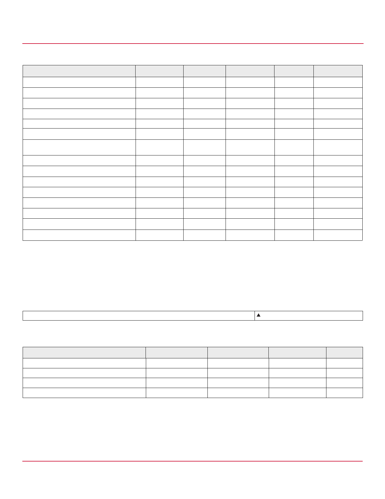
Absolute Maximum Ratings
Parameter
Symbol
Min
Max
Unit
Notes
Storage Temperature
Operating Temperature
Case Temperature
Junction Temperature
Lead Solder Temperature
Average Input Current
Peak Transient Input Current
(<1-μs pulse width, 300 pps)
Reverse Input Voltage
High Peak Output Current
Low Peak Output Current
Supply Voltage
Output Voltage
Input Power Dissipation
Output Power Dissipation
Total Power Dissipation
TS
–65
+150
°C
TA
–55
+125
°C
TC
—
+145
°C
TJ
—
+150
°C
—
260 for 10s
°C
IF AVG
—
25
mA
a
IF PK
—
1.0
A
VR
—
5
V
IOH (PEAK)
—
0.6
A
b
IOL (PEAK)
—
0.6
A
b
(VCC – VEE)
0
35
V
VO (PEAK)
0
VCC
V
PE
—
45
mW
a
PO
—
250
mW
c
PT
—
295
mW
d
a. No derating required with the typical case-to-ambient thermal resistance (θCA = 140°C/W). Refer to Figure 35.
b. Maximum pulse width = 10 μs, maximum duty cycle = 0.2%. This value is intended to allow for component tolerances for designs with IO peak minimum =
0.5A. See Applications Information for additional details on limiting IOH peak.
c. Derate linearly above 102°C free air temperature at a rate of 6 mW/°C with the typical case-to-ambient thermal resistance (θCA = 140°C/W). Refer to Figure 36.
d. Derate linearly above 102°C free air temperature at a rate of 6 mW/°C with the typical case-to-ambient thermal resistance (θCA = 140°C/W). Refer to Figure 35
and Figure 36.
ESD Classification
MIL-STD-883, Method 3015
, Class 1
Recommended Operating Conditions
Parameter
Power Supply Voltage
Input Current (ON)
Input Voltage (OFF)
Operating Temperature
Symbol
Min
(VCC – VEE)
15
IF(ON)
10
VF(OFF)
–3.0
TA
–55
Max
Unit
30
V
18
mA
0.8
V
125
°C
Broadcom
-4-
Share Link: 