5962-0420501HXA データシートの表示(PDF) - Broadcom Corporation
部品番号
コンポーネント説明
メーカー
5962-0420501HXA Datasheet PDF : 18 Pages
| |||
HCPL-5150 and HCPL-5151,
DLA SMD 5962-04205
Data Sheet
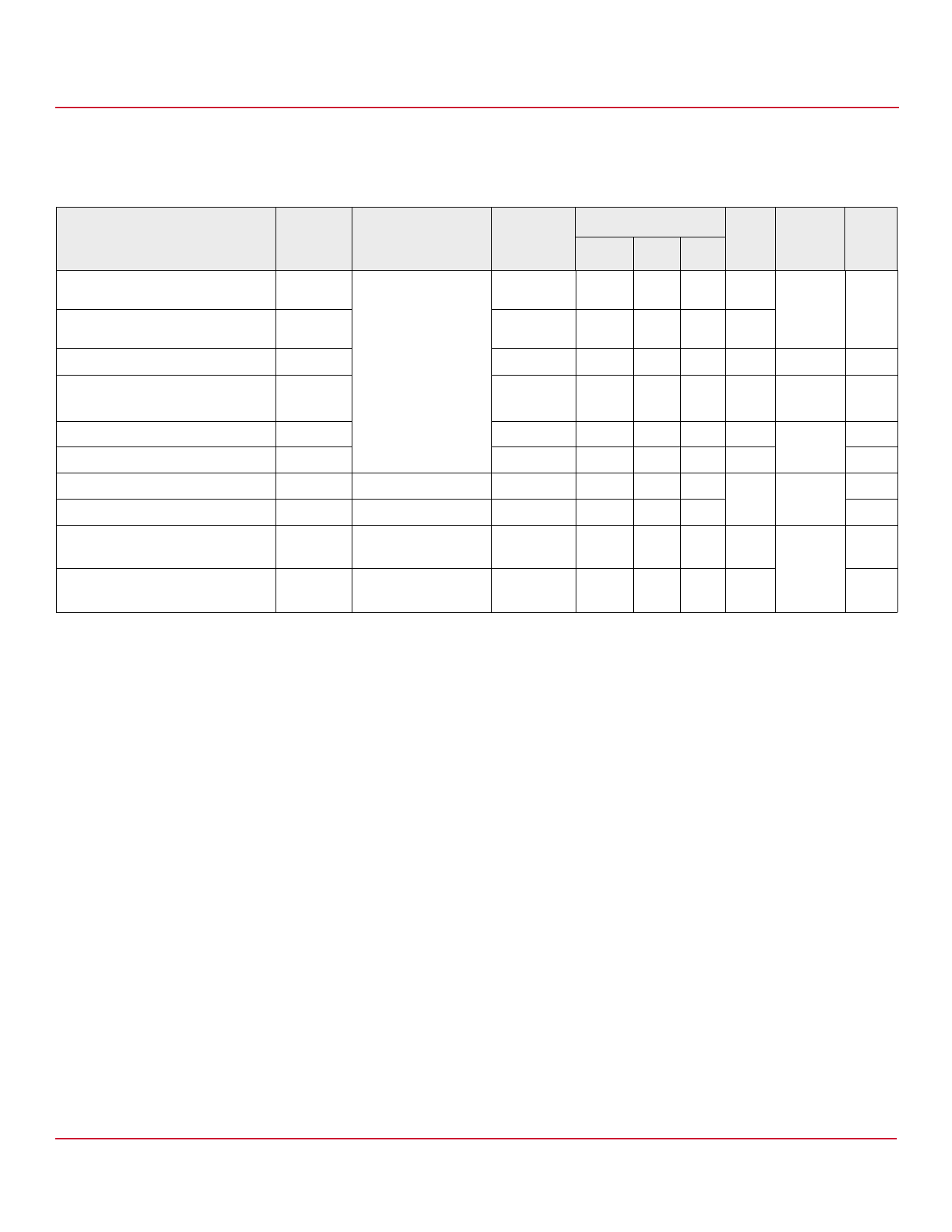
Switching Specifications (AC)
Over recommended operating conditions (TA = –55°C to +125°C, IF(ON) = 10 mA to 18 mA, VF(OFF) = –3.0V to 0.8V, VCC = 15V to 30V,
VEE = Ground) unless otherwise specified.
Parameter
Symbol
Test Conditions
Group A
Limits
Subgroupsa Min
Unit
Typb Max
Fig. Notes
Propagation Delay Time to High
Output Level
Propagation Delay Time to Low
Output Level
Pulse Width Distortion
tPLH
tPHL
PWD
Rg = 47Ω,
Cg = 3 nF,
f = 10 kHz,
Duty Cycle = 50%
9, 10, 11
9, 10, 11
9, 10, 11
0.10 0.30 0.50 μs 10, 11, 12, c
13, 14, 23
0.10 0.30 0.50 μs
—
— 0.3 μs
d
Propagation Delay Difference
Between Any Two Parts
PDD
(tPHL – tPLH)
9, 10, 11 –0.35 — 0.35 μs 33, 34
e
Rise Time
tr
—
0.1 — μs
23
Fall Time
tf
—
0.1 — μs
UVLO Turn On Delay
tUVLO ON VO > 5V, IF = 10 mA
—
0.8 — μs
22
UVLO Turn Off Delay
tUVLO OFF VO < 5V, IF = 10 mA
—
0.6 —
Output High-Level Common Mode
|CMH| IF = 10 mA, VCC = 30V
9
Transient Immunity
VCM = 1000V, TA = 25°C
10
— — kV/μs
24
f, g, h
Output Low-Level Common Mode
|CML| VCM = 1000V, VF = 0V,
9
10
— — kV/μs
f, i, h
Transient Immunity
VCC = 30V, TA = 25°C
a. Commercial parts receive 100% testing at 25°C (Subgroups 1 and 9). SMD and Class H parts receive 100% testing at 25°C, 125°C, and –55°C (Subgroups 1 and
9, 2 and 10, 3 and 11, respectively).
b. All typical values at TA = 25°C and VCC – VEE = 30V, unless otherwise noted.
c. This load condition approximates the gate load of a 1200V/25A IGBT.
d. Pulse Width Distortion (PWD) is defined as |tPHL – tPLH| for any given device.
e. The difference between tPHL and tPLH between any two HCPL-5150 parts under the same test condition.
f. Pins 1 and 4 need to be connected to LED common.
g. Common mode transient immunity in the high state is the maximum tolerable |dVCM/dt| of the common mode pulse, VCM, to assure that the output remains
in the high state (i.e., VO > 15.0V).
h. Parameters are tested as part of device initial characterization and after design and process changes. Parameters are guaranteed to limits specified for all lots
not specifically tested.
i. Common mode transient immunity in a low state is the maximum tolerable |dVCM/dt| of the common mode pulse, VCM, to assure that the output remains in
a low state (i.e., VO < 1.0V).
Broadcom
-6-
Share Link: 