HIP4086 データシートの表示(PDF) - Renesas Electronics
部品番号
コンポーネント説明
メーカー
HIP4086 Datasheet PDF : 17 Pages
| |||
HIP4086, HIP4086A
Absolute Maximum Ratings (Note 7)
Supply Voltage, VDD Relative to GND. . . . . . . . . . . . . . . . . . . . . -0.3V to 16V
Logic Inputs (xLI, xHI) . . . . . . . . . . . . . . . . . . . . . (GND - 0.3V) to VDD + 0.3V
Voltage on xHS . . . . . . . . . . . . . . -6V (Transient) to 85V (-40°C to +150°C)
Voltage on xHB . . . . . . . . . . . . . . . . . . . . . . . . . . . . (VxHS - 0.3V) to VxHS +VDD
Voltage on xLO . . . . . . . . . . . . . . . . . . . . . . . . . . . . . (VSS - 0.3V) to VDD +0.3V
Voltage on xHO . . . . . . . . . . . . . . . . . . . . . . . . . . . (VxHS - 0.3V) to VxHB +0.3V
Phase Slew Rate (on xHS) . . . . . . . . . . . . . . . . . . . . . . . . . . . . . . . . . . 20V/ns
Thermal Information
Thermal Resistance (Typical)
JA (°C/W) JC (°C/W)
SOIC Package (Notes 4, 6) . . . . . . . . . . . . .
75
22
SOIC Package HIP4086AABZ (Notes 5, 6)
51
22
PDIP* Package (Notes 4, 6) . . . . . . . . . . . .
70
29
Storage Temperature Range. . . . . . . . . . . . . . . . . . . . . . . .-65°C to +150°C
Operating Junction Temp Range . . . . . . . . . . . . . . . . . . . .-40°C to +150°C
Pb-Free Reflow Profile . . . . . . . . . . . . . . . . . . . . . . . . . . . . . . . . . . see TB493
Maximum Recommended Operating
Conditions
Supply Voltage, VDD Relative to GND. . . . . . . . . . . . . . . . . . . . . . . 7V to 15V
Logic Inputs (xLI, xHI) . . . . . . . . . . . . . . . . . . . . . . . . . . . . . . . . . . . 0V to VDD
Voltage on xHB . . . . . . . . . . . . . . . . . . . . . . . . . . . . . . . . . . . . . . . VxHS + VDD
Voltage on xHS . . . . . . . . . . . . . . . . . . . . . . . . . . . . . . . . . . . . . . . . . 0V to 80V
Ambient Temperature Range . . . . . . . . . . . . . . . . . . . . . . .-40°C to +125°C
Junction Temperature Range . . . . . . . . . . . . . . . . . . . . . . .-40°C to +150°C
RDEL range . . . . . . . . . . . . . . . . . . . . . . . . . . . . . . . . . . . . . . . 10kΩ to 100kΩ
*Pb-free PDIPs can be used for through-hole wave solder processing only.
They are not intended for use in Reflow solder processing applications.
CAUTION: Do not operate at or near the maximum ratings listed for extended periods of time. Exposure to such conditions may adversely impact product
reliability and result in failures not covered by warranty.
NOTES:
4. JA is measured with the component mounted on a low effective thermal conductivity test board in free air. See Tech Brief TB379 for details.
5. JA is measured with the component mounted on a high effective thermal conductivity test board in free air. See Tech Brief TB379 for details.
6. For JC, the “case temp” location is taken at the package top center.
7. Replace x with A, B, or C.
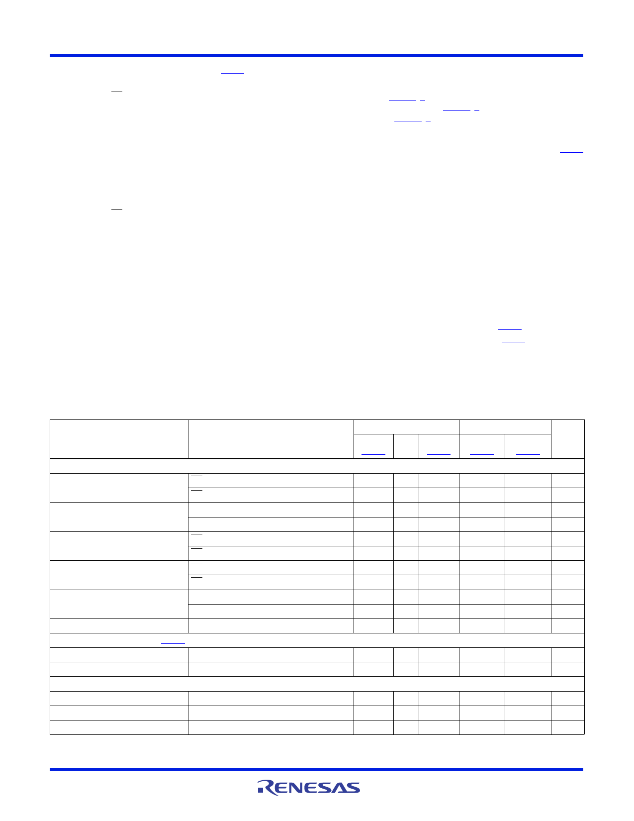
DC Electrical Specifications VDD = VxHB = 12V, VSS = VxHS = 0V, RDEL = 20k, RUV = , Gate Capacitance (CGATE) = 1000pF, unless
otherwise specified. Boldface limits apply across the operating junction temperature range, -40°C to +150°C.
PARAMETER
TEST CONDITIONS
TJ = +25°C
MIN
MAX
(Note 9) TYP (Note 9)
TJ = -40°C TO +150°C
MIN
(Note 9)
MAX
(Note 9)
UNIT
SUPPLY CURRENTS
VDD Quiescent Current
xHI = 5V, xLI = 5V (HIP4086)
xHI = 5V, xLI = 5V (HIP4086A)
2.7 3.4 5.1
2.3 2.8 3.1
1.96
1.8
5.3
mA
3.3
mA
VDD Operating Current
f = 20kHz, 50% Duty Cycle (HIP4086)
f = 20kHz, 50% Duty Cycle (HIP4086A)
5.4 8.25 13
4
13.5
mA
3.1 4.0 4.6
2.7
5.1
mA
xHB On Quiescent Current
xHI = 0V (HIP4086)
-
40 110
-
140
µA
xHI = 0V (HIP4086A)
-
90 115
-
225
µA
xHB Off Quiescent Current
xHB Operating Current
xHI = VDD (HIP4086)
xHI = VDD (HIP4086A)
f = 20kHz, 50% Duty Cycle (HIP4086)
0.6 0.8 1.3
0.5
1.4
mA
0.8 1.0 1.2
0.7
1.25
mA
0.7 0.9 1.3
-
2.0
mA
f = 20kHz, 50% Duty Cycle (HIP4086A)
0.8 0.9 1.1
-
1.25
mA
xHB, xHS Leakage Current
VxHS = 80V, VxHB = 93V
Charge Pump, HIP4086 Only, (Note 8)
7
30
45
-
50
µA
QPUMP Output Voltage
QPUMP Output Current
UNDERVOLTAGE PROTECTION
No Load
VxHS = 12V, VxHB = 22V
11 12.5 14.6
10
14.75
V
40 100 160
-
185
µA
VDD Rising Undervoltage Threshold
VDD Falling Undervoltage Threshold
Minimum Undervoltage Threshold
RUV open
RUV open
RUV = VDD
6.2 7.1 8.0
6.1
5.75 6.6 7.5
5.6
5
6.2 6.8
4.8
8.1
V
7.6
V
6.9
V
FN4220 Rev 1.00
January 12, 2017
Page 5 of 17
Share Link: 