DMG3407SSN データシートの表示(PDF) - Diodes Incorporated.
部品番号
コンポーネント説明
メーカー
DMG3407SSN Datasheet PDF : 7 Pages
| |||
DMG3407SSN
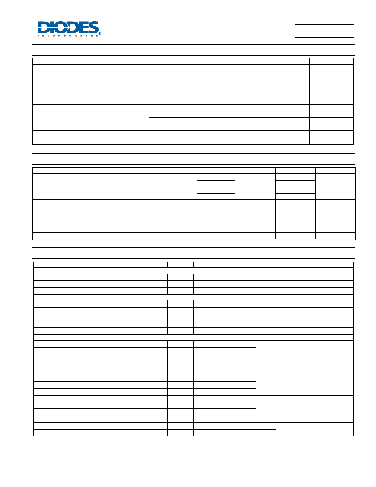
Maximum Ratings (@TA = +25°C, unless otherwise specified.)
Drain-Source Voltage
Gate-Source Voltage
Characteristic
Continuous Drain Current (Note 6) VGS = -10V
Continuous Drain Current (Note 6) VGS = -4.5V
Pulsed Drain Current (10s Pulse, Duty Cycle = 1%)
Maximum Body Diode Forward Current (Note 6)
Steady
State
t<10s
Steady
State
t<10s
TA = +25°C
TA = +70°C
TA = +25°C
TA = +70°C
TA = +25°C
TA = +70°C
TA = +25°C
TA = +70°C
Symbol
VDSS
VGSS
ID
ID
ID
ID
IDM
IS
Value
-30
±20
-4.0
-3.2
-4.6
-3.6
-3.3
-2.6
-3.9
-3.1
-30
-2.0
Unit
V
V
A
A
A
A
A
A
Thermal Characteristics (@TA = +25°C, unless otherwise specified.)
Total Power Dissipation (Note 5)
Characteristic
Thermal Resistance, Junction to Ambient (Note 5)
Total Power Dissipation (Note 6)
Thermal Resistance, Junction to Ambient (Note 6)
Thermal Resistance, Junction to Case (Note 6)
Operating and Storage Temperature Range
TA = +25°C
TA = +70°C
Steady state
t<10s
TA = +25°C
TA = +70°C
Steady state
t<10s
Symbol
PD
RJA
PD
RJA
RJC
TJ, TSTG
Value
1.1
0.7
166
118
1.8
1.1
98
71
18
-55 to +150
Unit
W
°C/W
W
°C/W
°C
Electrical Characteristics (@ TA = +25°C, unless otherwise stated.)
Characteristic
OFF CHARACTERISTICS (Note 7)
Drain-Source Breakdown Voltage
Zero Gate Voltage Drain Current, TJ = +25°C
Gate-Source Leakage
ON CHARACTERISTICS (Note 7)
Gate Threshold Voltage
Static Drain-Source On-Resistance
Forward Transfer Admittance
Diode Forward Voltage
DYNAMIC CHARACTERISTICS (Note 8)
Input Capacitance
Output Capacitance
Reverse Transfer Capacitance
Gate Resistance
Total Gate Charge
Total Gate Charge
Gate-Source Charge
Gate-Drain Charge
Turn-On Delay Time
Turn-On Rise Time
Turn-Off Delay Time
Turn-Off Fall Time
Reverse Recovery Time
Reverse Recovery Charge
Symbol
BVDSS
IDSS
IGSS
VGS(TH)
RDS(ON)
|Yfs|
VSD
Ciss
Coss
Crss
Rg
Qg
Qg
Qgs
Qgd
tD(ON)
tR
tD(OFF)
tF
tRR
QRR
Min
-30
-
-
-1.0
-
-
-
-
466
80
47
2
10.6
5.2
1.3
1.1
-
-
-
-
6.8
5.5
Typ
-
-
-
-1.5
39
56
8.2
-0.75
582
114
76
5
13.3
6.5
1.7
1.9
6.0
12.9
35.4
30.7
8.5
7.0
Max
-
-1
±100
-2.1
50
72
-
-1.1
700
148
105
8
16
8.5
2
2.7
-
-
-
-
10.2
8.5
Unit
Test Condition
V VGS = 0V, ID = -250μA
A VDS = -30V, VGS = 0V
nA VGS = ±20V, VDS = 0V
V VDS = VGS, ID = -250μA
mΩ VGS = -10V, ID = -4.1A
VGS = -4.5V, ID = -3.0A
S VDS = -5V, ID = -4A
V VGS = 0V, IS = -1A
pF
VDS = -15V, VGS = 0V,
f = 1.0MHz
Ω VDS = 0V, VGS = 0V, f = 1MHz
VGS = -10V, VDS = -15V, ID = -4A
nC
VGS = -4.5V, VDS = -15V,ID = -4A
ns VGS = -10V, VDS = -15V,
RL = 3.6Ω, RG = 3Ω
ns
nC IF = 4A, di/dt = 100A/μs
Notes:
5. Device mounted on FR-4 PCB with minimum recommended pad layout, single sided. The power dissipation PD is based on t<10s RJA.
6. Device mounted on 1” x 1” FR-4 PCB with high coverage 2 oz. copper, single sided. The power dissipation PD is based on t<10s RJA.
7. Short duration pulse test used to minimize self-heating effect.
8. Guaranteed by design. Not subject to production testing.
DMG3407SSN
Document number: DS35135 Rev. 7 - 2
2 of 7
www.diodes.com
February 2017
© Diodes Incorporated
Share Link: 