ACPL-P484-560E データシートの表示(PDF) - Broadcom Corporation
部品番号
コンポーネント説明
メーカー
ACPL-P484-560E
Broadcom Corporation

ACPL-P484-560E Datasheet PDF : 13 Pages
| |||
ACPL-M484/P484/W484
Data Sheet
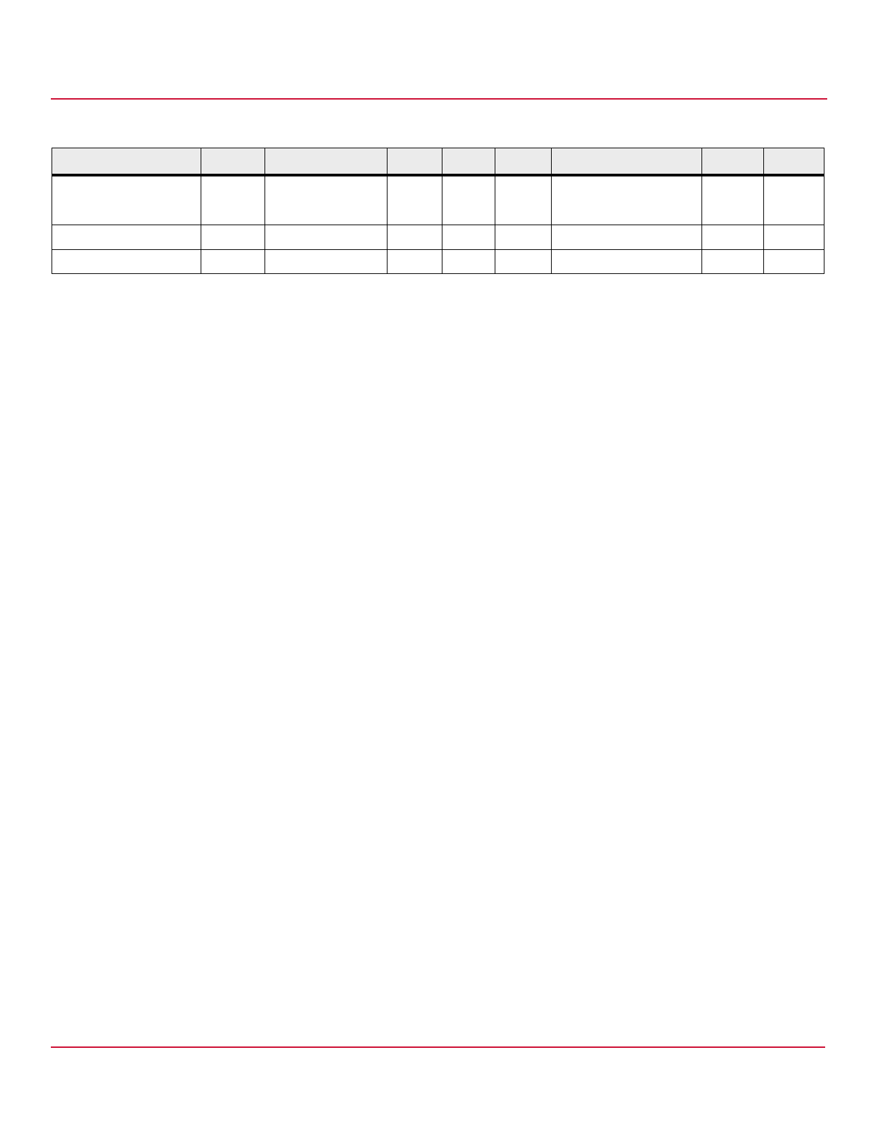
Package Characteristics
Parameter
Symbol
Min.
Typ. Max. Unit
Test Conditions
Fig.
Note
Input-Output Momentary VISO
Withstand Voltagea
3750
(ACPL-M484/P484)
5000 (ACPL-W484)
VRMS
RH < 50%, t = 1 min.
5, 8
TA = 25°C
Input-Output Resistance
RI-O
1012
Ω
VI-O = 500VDC
5
Input-Output Capacitance CI-O
0.6
pF
f = 1 MHz, VI-O = 0VDC
5
a. The Input-Output Momentary Withstand Voltage is a dielectric voltage rating that should not be interpreted as an input-output continuous voltage rating.
For the continuous voltage rating refer to the IEC/EN/DIN EN 60747-5-5 Insulation Characteristics Table (if applicable).
UVLO
Figure 10 and Figure 11 show typical output waveforms during Power-up and Power-down processes.
Notes:
1. Derate total package power dissipation, PT, linearly above 70°C free-air temperature at a rate of 4.5 mW/°C (ACPL-P484/W484) and linearly
above 85°C free-air temperature at a rate of 0.75 mW/°C (ACPL-M484).
2. Detector requires a VCC of 4.5V or higher for stable operation as output might be unstable if VCC is lower than 4.5V. Be sure to check the power
ON/OFF operation other than the supply current.
3. Duration of output short circuit time should not exceed 500 μs.
4. Input capacitance is measured between pin 1 and pin 3.
5. Device considered a two-terminal device: pins 1, 2, and 3 shorted together and pins 4, 5, and 6 shorted together.
6. The tPLH propagation delay is measured from the 50% point on the leading edge of the input pulse to the 1.3V point on the leading edge of
the output pulse. The tPHL propagation delay is measured from the 50% point on the trailing edge of the input pulse to the 1.3 V point on
the trailing edge of the output pulse.
7. CMH is the maximum slew rate of the common mode voltage that can be sustained with the output voltage in the logic high state, VO > 2.0V.
CML is the maximum slew rate of the common mode voltage that can be sustained with the output voltage in the logic low state, VO < 0.8V.
Note: Equal value split resistors (Rin/2) must be used at both ends of the LED.
8. In accordance with UL 1577, each optocoupler is proof tested by applying an insulation test voltage. 4500VRMS for one second (leakage
detection current limit, II-O ≤ 5 μA). This test is performed before the 100% production test for partial discharge (Method b) shown in the
IEC/EN/DIN EN 60747-5-5 Insulation Characteristics Table, if applicable.
9. Pulse Width Distortion (PWD) is defined as |tPHL – tPLH| for any given device.
10. The difference of tPLH and tPHL between any two devices under the same test condition.
11. Use of a 0.1 μF bypass capacitor connected between pins VCC and Ground is recommended.
Broadcom
-8-
Share Link: