HCPL-5200-100 データシートの表示(PDF) - Broadcom Corporation
部品番号
コンポーネント説明
メーカー
HCPL-5200-100 Datasheet PDF : 15 Pages
| |||
HCPL-520x, HCPL-523x, HCPL-623x, HCPL-625x, 5962-88768 and 5962-88769
Data Sheet
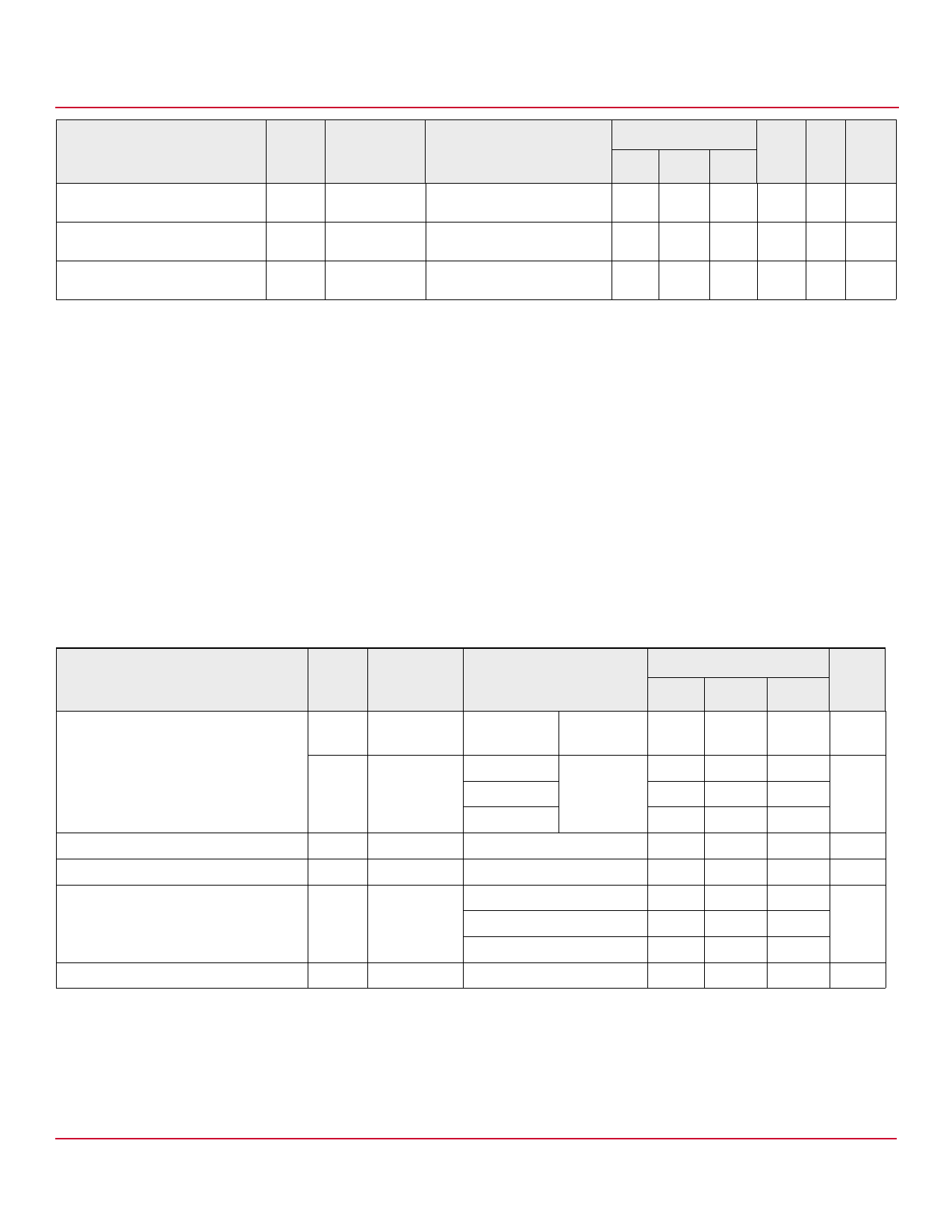
Electrical Characteristics - Single Channel Product Only
Parameter
Group A
Symbol Sub-groupsa
Test Conditions
Limits
Unit Fig Notes
Min Typb Max
Logic Low Common Mode
Transient Immunity
Propagation Delay Time to Logic
Low
Propagation Delay Time to Logic
High
|CML|
tPHL
tPLH
9, 10, 11
9, 10, 11
9, 10, 11
IF = 0 mA, VCM = 50VP-P
1000 10,000
V/μs 9 c, g, h
— 173 350 ns 5, 6 c, i
— 118 350 ns 5, 6 c, i
a. Commercial parts receive 100% testing at 25°C (Subgroups 1 and 9). SMD, Class H and Class K parts receive 100% testing at 25, 125, and –55°C (Subgroups 1
and 9, 2 and 10, 3 and 11, respectively).
b. All typical values are at VCC = 5V, TA = 25°C, IF(ON) = 5 mA unless otherwise specified.
c. Each channel of a multichannel device.
d. Duration of output short circuit time not to exceed 10 ms.
e. All devices are considered two-terminal devices: measured between all input leads or terminals shorted together and all output leads or terminals shorted
together.
f. This is a momentary withstand test, not an operating condition.
g. CML is the maximum rate of rise of the common mode voltage that can be sustained with the output voltage in the logic low state (VO < 0.8V). CMH is the
maximum rate of fall of the common mode voltage that can be sustained with the output voltage in the logic high state (VO >2.0V).
h. Parameters are tested as part of device initial characterization and after design and process changes. Parameters guaranteed to limits specified for all lots not
specifically tested.
i. tPHL propagation delay is measured from the 50% point on the leading edge of the input pulse to the 1.3V point on the leading edge of the output pulse. The
tPLH propagation delay is measured from the 50% point on the trailing edge of the input pulse to the 1.3V point on the trailing edge of the output pulse.
Electrical Characteristics - Single Channel Product Only
TA = –55°C to +125°C, 4.5V ≤ VCC ≤ 20V, 2 mA ≤ IF(ON) ≤ 8 mA, 0V ≤ VF(OFF) ≤ 0.8V, unless otherwise specified.
Parameter
Group A,
Symbol Sub-groupsa
Test Conditions
Limits
Unit
Min
Typb
Max
High Impedance State Output Current
IOZL
IOZH
Logic High Enable Voltage
VEH
Logic Low Enable Voltage
VEL
Logic High Enable Current
IEH
Logic Low Enable Current
IEL
1, 2, 3
1, 2, 3
1, 2, 3
1, 2, 3
1, 2, 3
1, 2, 3
VO = 0.4V
VEN = 2V,
—
—
–20
μA
VF = 0V
VO = 2.4V
VEN = 2V,
—
—
20
μA
VO = 5.5V
IF = 8 mA
—
—
100
VO = 20V
—
—
500
2.0
V
—
—
0.8
V
VEN = 2.7V
VEN = 5.5V
VEN = 20V
VEN = 0.4V
—
—
20
μA
—
—
100
—
0.004
250
—
—
–0.32 mA
a. Commercial parts receive 100% testing at 25°C (Subgroups 1 and 9). SMD, Class H and Class K parts receive 100% testing at 25, 125, and –55°C (Subgroups
1 and 9, 2 and 10, 3 and 11, respectively).
b. All typical values are at VCC = 5V, TA = 25°C, IF(ON) = 5 mA unless otherwise specified.
Broadcom
-9-
Share Link: 