ML9213 データシートの表示(PDF) - LAPIS Semiconductor Co., Ltd.
部品番号
コンポーネント説明
メーカー
ML9213
LAPIS Semiconductor Co., Ltd.

ML9213 Datasheet PDF : 19 Pages
| |||
1Semiconductor
FEDL9213-01
ML9213
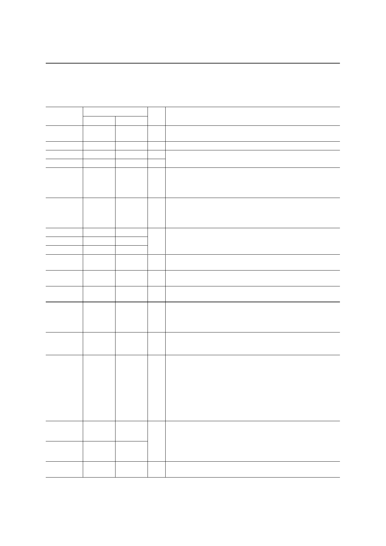
PIN DESCRIPTIONS
Symbol
VDISP
VDD
D-GND
L-GND
SEG1 to 37
SEG38 to 56
GRID1
GRID2
GRID3
CS
CLOCK
DATA IN
DUP/TRI
M/S
DIM IN
SYNC IN1
SYNC IN2
Pin
Type
ML9213GA ML9213GP
65, 80
63, 78 —
25
24, 40
33
23
—
22, 38 —
31
—
42 to 64, 40 to 62,
66 to 79 64 to 77
O
1 to 19
79, 80,
1 to 17
O
20
18
21
19
O
22
20
29
27
I
30
28
I
31
29
I
35
33
I
36
34
I
26
24
I
27
25
I
28
26
Description
Power supply pins for VFD driver circuit.
These should be connected externally.
Power supply pin for logic drive.
D-GND is ground pin for the VFD driver circuit. L-GND is ground
pin for the logic circuit. These should be connected externally.
Segment (anode) signal output pins for a VFD tube. These pins
can be directly connected to the VFD tube. External circuit is not
required.
IOH d –5 mA
Segment (anode) signal output pins for a VFD tube. These pins
can be directly connected to the VFD tube. External circuit is not
required.
IOH d –10 mA
Inverted Grid signal output pins. Since these pins are connected
to the pre-driver, an external circuit is required.
IOL d 10 mA
Chip select input pin.
Data is not transferred when CS is set to a Low level.
Shift clock input pin.
Serial data shifts at the rising edge of the CLOCK.
Serial data input pin (positive logic). Data is input to the shift
register at the rising edge of the CLOCK signal.
Duplex/Triplex operation select input pin.
Duplex (1/2 duty) operation is selected when this pin is set to VDD.
Triplex (1/3 duty) operation is selected when this pin is set to L-
GND.
Master/Slave mode select input pin.
Master mode is selected when this pin is set to VDD.
Slave mode is selected when this pin is set to L-GND.
Dimming pulse input.
When the slave mode is selected, connect this pin to the master
side DIM OUT pin. The pulse width of all the segment outputs is
controlled by an input pulse width of DIM IN. When the master
mode is selected, input to this pin is ignored; therefore, connect
this pin to VDD or L-GND. The pulse width of all the segment
outputs is controlled by the built-in digital dimming circuit, and the
pulse width of all the grid outputs is controlled by the internal
timing generator.
Synchronous signal input.
When the slave mode is selected, connect these pins to the
master side SYN COUT1 and 2 pins.
When the master mode is selected, input to these pins is ignored;
therefore, connect these pins to VDD or L-GND.
DIM OUT
39
37
O
Dimming pulse output.
Connect this pin to the slave side DIM IN pin.
5/19
Share Link: