EL5412 データシートの表示(PDF) - Renesas Electronics
部品番号
コンポーネント説明
メーカー
EL5412 Datasheet PDF : 8 Pages
| |||
EL5412
Where:
• i = Channel 1 to 4
• VS = Total supply voltage
• ISMAX = Maximum supply current per amplifier
• VOUTi = Maximum output voltage of the application
• ILOADi = Load current
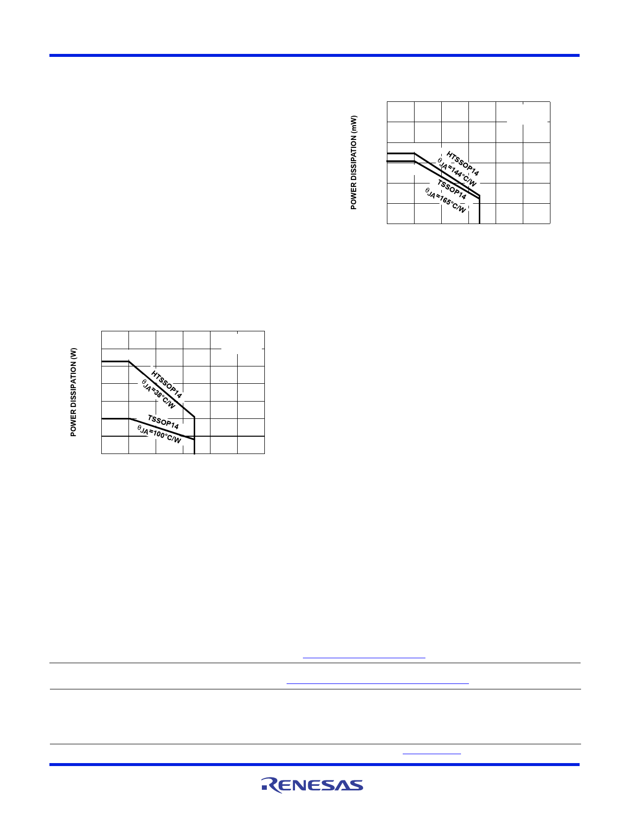
If we set the two PDMAX equations equal to each other, we
can solve for RLOADi to avoid device overheat. Figure 10
and Figure 11 provide a convenient way to see if the device
will overheat. The maximum safe power dissipation can be
found graphically, based on the package type and the
ambient temperature. By using the previous equation, it is a
simple matter to see if PDMAX exceeds the device's power
derating curves. To ensure proper operation, it is important
to observe the recommended derating curves shown in
Figures 10 and 11.
JEDEC JESD51-7 HIGH EFFECTIVE THERMAL
CONDUCTIVITY TEST BOARD - HTSSOP
EXPOSED DIEPAD SOLDERED TO PCB PER
JESD51-5
3.5
MAX
3
2.632W
TJ=125°C
2.5
2
1.5
1.0W
1
0.5
JA =H3T8S°CSO/WP14
JAT=S1S00O°PC1/W4
0
0
25
50
75 85 100 125 150
AMBIENT TEMPERATURE (°C)
FIGURE 10. PACKAGE POWER DISSIPATION vs AMBIENT
TEMPERATURE
PACKAGE MOUNTED ON A JEDEC JESD51-3
LOW EFFECTIVE THERMAL CONDUCTIVITY
TEST BOARD
1200
MAX
1000
TJ=125°C
800
694mW
600
606mW
400
200
JA =T1JSA6S5H=O°1TC4PS/41WS°4OCP/W14
0
0
25
50
75 85 100 125 150
AMBIENT TEMPERATURE (°C)
FIGURE 11. PACKAGE POWER DISSIPATION vs AMBIENT
TEMPERATURE
Unused Amplifiers
It is recommended that any unused amplifiers be configured
as a unity gain follower. The inverting input should be directly
connected to the output and the non-inverting input tied to
the ground plane.
Power Supply Bypassing and Printed Circuit
Board Layout
The EL5412 can provide gain at high frequency. As with any
high-frequency device, good printed circuit board layout is
necessary for optimum performance. Ground plane
construction is highly recommended, lead lengths should be
as short as possible and the power supply pins must be well
bypassed to reduce the risk of oscillation. For normal single
supply operation, where the VS- pin is connected to ground,
a 0.1µF ceramic capacitor should be placed from VS+ to pin
to VS- pin. A 4.7µF tantalum capacitor should then be
connected in parallel, placed in the region of the amplifier.
One 4.7µF capacitor may be used for multiple devices. This
same capacitor combination should be placed at each
supply pin to ground if split supplies are to be used.
© Copyright Intersil Americas LLC 2003-2004. All Rights Reserved.
All trademarks and registered trademarks are the property of their respective owners.
For additional products, see www.intersil.com/en/products.html
Intersil products are manufactured, assembled and tested utilizing ISO9001 quality systems as noted
in the quality certifications found at www.intersil.com/en/support/qualandreliability.html
Intersil products are sold by description only. Intersil may modify the circuit design and/or specifications of products at any time without notice, provided that such
modification does not, in Intersil's sole judgment, affect the form, fit or function of the product. Accordingly, the reader is cautioned to verify that datasheets are
current before placing orders. Information furnished by Intersil is believed to be accurate and reliable. However, no responsibility is assumed by Intersil or its
subsidiaries for its use; nor for any infringements of patents or other rights of third parties which may result from its use. No license is granted by implication or
otherwise under any patent or patent rights of Intersil or its subsidiaries.
For information regarding Intersil Corporation and its products, see www.intersil.com
FN7394 Rev 1.00
December 22, 2004
Page 8 of 8
Share Link: 