LH28F400SU-LC гғҮгғјгӮҝгӮ·гғјгғҲгҒ®иЎЁзӨәпјҲPDFпјү - Sharp Electronics
йғЁе“Ғз•ӘеҸ·
гӮігғігғқгғјгғҚгғігғҲиӘ¬жҳҺ
гғЎгғјгӮ«гғј
LH28F400SU-LC Datasheet PDF : 37 Pages
| |||
LH28F400SU-LC
4M (512K Г— 8, 256K Г— 16) Flash Memory
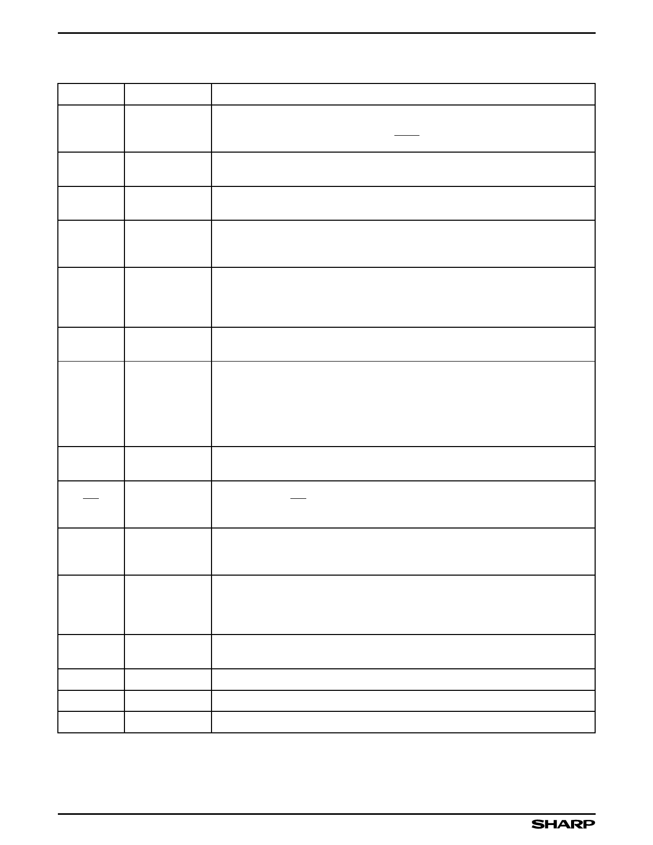
PIN DESCRIPTION
SYMBOL
TYPE
NAME AND FUNCTION
DQ15 - A1 INPUT
A0 - A12 INPUT
BYTE-SELECT ADDRESSES: Selects between high and low byte when device is in
x8 mode. This address is latched in x8 Data Writes. Not used in x16 mode (i.e., the
DQ15/A1 input buffer is turned off when BYTE is high).
WORD-SELECT ADDRESSES: Select a word within one 16K block. These
addresses are latched during Data Writes.
A13 - A17 INPUT
BLOCK-SELECT ADDRESSES: Select 1 of 32 Erase blocks. These addresses are
latched during Data Writes, Erase and Lock-Block operations.
DQ0 - DQ7
INPUT/OUTPUT
LOW-BYTE DATA BUS: Inputs data and commands during CUI write cycles.
Outputs array, buffer, identifier or status data in the appropriate Read mode.
Floated when the chip is de-selected or the outputs are disabled.
DQ8 - DQ15
CE В»
INPUT/OUTPUT
INPUT
HIGH-BYTE DATA BUS: Inputs data during x16 Data Write operations. Outputs
array, buffer or identifier data in the appropriate Read mode; not used for Status
register reads. Floated when the chip is de-selected or the outputs are disabled.
DQ15/A1 is address.
CHIP ENABLE INPUT: Activate the deviceвҖҷs control logic, input buffers, decoders
and sense amplifiers. CEВ» must be low to select the device.
RP В»
INPUT
RESET/POWER-DOWN: RP В» low places the device in a Deep Power-Down state. All
circuits that burn static power, even those circuits enabled in standby mode, are
turned off. When returning from Deep Power-Down, a recovery time of 750 ns is
required to allow these circuits to power-up. When RPВ» goes low, any current or
pending WSM operation(s) are terminated, and the device is reset. All Status
registers return to ready (with all status flags cleared).
OE В»
INPUT
OUTPUT ENABLE: Gates device data through the output buffers when low. The
outputs float to tri-state off when OEВ» is high.
WE
INPUT
WRITE ENABLE: Controls access to the CUI, Data Queue Registers and Address
Queue Latches. WE is active low, and latches both address and data (command or
array) on its rising edge.
RY В»/BY В»
OPEN DRAIN
OUTPUT
READY/BUSY: Indicates status of the internal WSM. When low, it indicates that the
WSM is busy performing an operation. When the WSM is ready for new operation or
Erase is Suspended, or the device is in deep power-down mode RYВ»/BY В» pin is floated.
BYTE INPUT
VPP
SUPPLY
BYTE ENABLE: BYTE low places device in x8 mode. All data is then input or
output on DQ0 - DQ7, and DQ8 - DQ15 float. Address A1 selects between the high
and low byte. BYTE high places the device in x16 mode, and turns off the A1 input
buffer. Address A0, then becomes the lowest order address.
ERASE/WRITE POWER SUPPLY (5.0 V Вұ0.5 V): For erasing memory array blocks
or writing words/bytes into the flash array.
VCC
GND
SUPPLY
SUPPLY
DEVICE POWER SUPPLY (3.0 V Вұ0.3 V): Do not leave any power pins floating.
GROUND FOR ALL INTERNAL CIRCUITRY: Do not leave any ground pins floating.
NC
NO CONNECT: No internal connection to die, lead may be driven or left floating.
4
Share Link: 