ISL43120 データシートの表示(PDF) - Renesas Electronics
部品番号
コンポーネント説明
メーカー
ISL43120 Datasheet PDF : 13 Pages
| |||
ISL43120, ISL43121, ISL43122
Electrical Specifications - 12V Supply V+ = +10.8V to +13V, GND = 0V, VINH = 2.4V, VINL = 0.8V (Note 8), unless otherwise
specified. Boldface limits apply across the operating temperature range, -40°C to +85°C. (Continued)
PARAMETER
TEST CONDITIONS
TEMP
MIN
MAX
(°C) (Notes 9, 10) TYP (Notes 9, 10) UNIT
DIGITAL INPUT CHARACTERISTICS
Input Voltage Low, VINL
Full
-
-
0.8
V
Input Voltage High, VINH
Full
4
-
-
V
Input Current, IINH, IINL
V+ = 13V, VIN = 0V or V+
Full
-1
-
1
µA
NOTES:
8. VIN = input voltage to perform proper function.
9. The algebraic convention, whereby the most negative value is a minimum and the most positive a maximum, is used in this data sheet.
10. Compliance to datasheet limits is assured by one or more methods: production test, characterization and/or design.
11. Limits established by characterization and are not production tested.
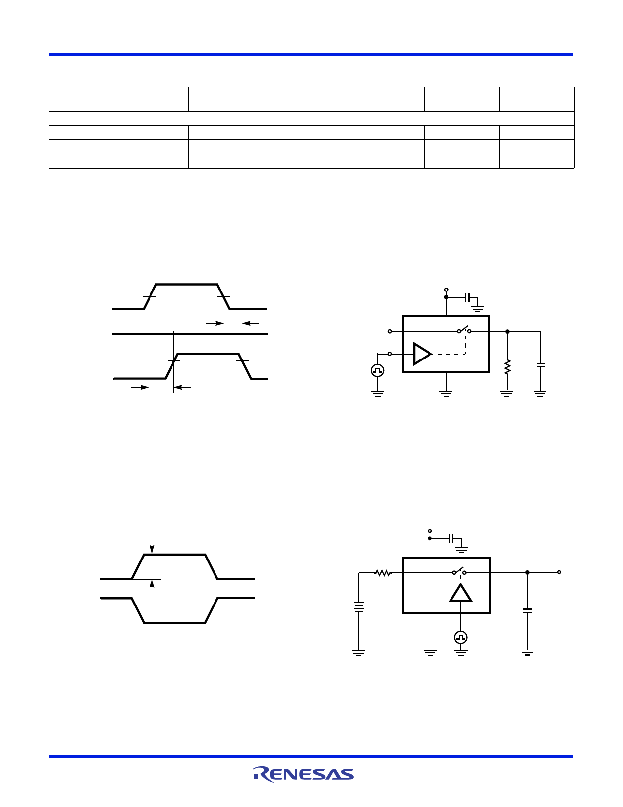
Test Circuits and Waveforms
3V OR 4V
LOGIC
INPUT
0V
SWITCH
INPUT
VNO
SWITCH
OUTPUT 0V
50%
tOFF
VOUT
90%
tON
tr < 20ns
tf < 20ns
90%
V+
C
SWITCH
INPUT
LOGIC
INPUT
NO OR NC
IN
GND
COM
VOUT
RL
CL
1k 35pF
Logic input waveform is inverted for switches that have the opposite
logic sense.
FIGURE 1A. MEASUREMENT POINTS
Repeat test for all switches. CL includes fixture and stray
capacitance.
VOUT = V(NO or NC) R-----L----R+----L-r---O----N--
FIGURE 1B. TEST CIRCUIT
FIGURE 1. SWITCHING TIMES
V+
C
SWITCH
OUTPUT
VOUT
LOGIC ON
INPUT
VOUT
OFF
Q = VOUT x CL
V+
ON
0V
RG
NO OR NC
COM
VG
GND
IN
LOGIC
INPUT
FIGURE 2A. MEASUREMENT POINTS
FIGURE 2. CHARGE INJECTION
FIGURE 2B. TEST CIRCUIT
VOUT
CL
FN6033 Rev 7.00
Aug 17, 2015
Page 6 of 13
Share Link: 