ISL88041 データシートの表示(PDF) - Renesas Electronics
部品番号
コンポーネント説明
メーカー
ISL88041 Datasheet PDF : 7 Pages
| |||
ISL88041
Absolute Maximum Ratings
VDD . . . . . . . . . . . . . . . . . . . . . . . . . . . . . . . . . . . . . . . . . . . . . +5.5V
VMON, RST, MR . . . . . . . . . . . . . . . . . . . . . . . . . -0.3V to VDD+0.3V
ESD Classification . . . . . . . . . . . . . . . . . . . . . . . . . . . . . . 4kV (HBM)
Operating Conditions
VDD Supply Voltage Range . . . . . . . . . . . . . . . . . . . . . +2.7V to +4V
Temperature Range (TA) . . . . . . . . . . . . . . . . . . . . . .-40°C to +85°C
Thermal Information
Thermal Resistance (Typical, Note 1)
JA (°C/W)
8 Ld SOIC . . . . . . . . . . . . . . . . . . . . . . . . . . . . . . . .
108
Maximum Junction Temperature . . . . . . . . . . . . . . . . . . . . . . +150°C
Maximum Storage Temperature Range . . . . . . . . . .-65°C to +150°C
Pb-Free Reflow Profile. . . . . . . . . . . . . . . . . . . . . . . . .see link below
http://www.intersil.com/pbfree/Pb-FreeReflow.asp
CAUTION: Do not operate at or near the maximum ratings listed for extended periods of time. Exposure to such conditions may adversely impact product reliability and
result in failures not covered by warranty.
NOTES:
1. JA is measured in free air with the component mounted on a high effective thermal conductivity test board. See Tech Brief TB379 for details.
2. All voltages are relative to GND, unless otherwise specified.
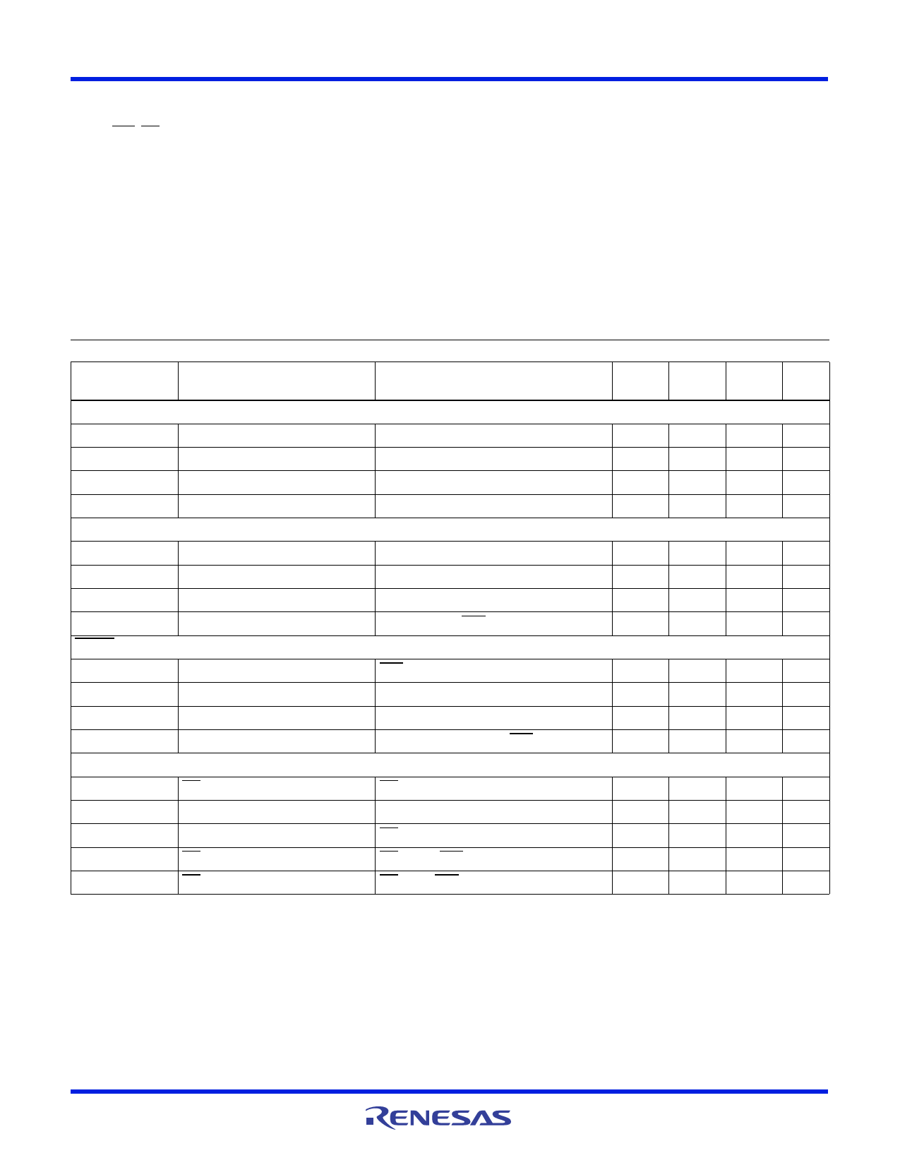
Electrical Specifications VDD = 3.3V, TA = TJ = -40°C to +85°C, Unless Otherwise Specified.
SYMBOL
PARAMETER
TEST CONDITIONS
MIN
(Note 3)
TYP
MAX
(Note 3) UNIT
BIAS
VDD
IDD
VDD_LO
VDD_LOR
VMON
Supply Voltage Range
VDD Supply Current
VDD Lock Out
VDD Lock Out Reset
VMON > VREF
VDD low to high
VDD high to low
2.7
4.0
V
165
1000
µA
2.6
V
2.4
V
VREF
VREFHYST
VREF_RNG
tFIL
RESET
Adj. Reset Threshold Voltage
Hysteresis of VREF
Range
Glitch Filter Duration
VREF (max) - VREF (min)
VMON glitch to RST low Filter
619
635
651
mV
10
mV
1.8
mV
30
µs
IPD
RPU
VOL
tRPD
MANUAL RESET
Pull-down Current
Internal Pull-up Resistance
Output Low
VTH to Reset Asserted Delay
RST = 0.5V
VDD = 1V
Last valid input = VTH to RST release
2
mA
20
k
0.05
0.1
V
1.5
µs
VMR
MR Input Voltage
MR low to high threshold
0.4VDD 0.5VDD 0.6VDD
V
VMRHYST
Hysteresis of VMR
0.065
V
IPU
Pull-up Current
MR = 0.5V
10
µA
tMD
MR to Deassert Reset Out Delay MR high to RST release
50
ns
tMR
MR to Assert Reset Out Delay
MR low to RST pulling low
15
ns
NOTE:
3. Parameters with MIN and/or MAX limits are 100% tested at +25°C, unless otherwise specified. Temperature limits established by characterization
and are not production tested.
FN9229 Rev 2.00
April 29, 2010
Page 3 of 7
Share Link: 