ISL88705 гғҮгғјгӮҝгӮ·гғјгғҲгҒ®иЎЁзӨәпјҲPDFпјү - Renesas Electronics
йғЁе“Ғз•ӘеҸ·
гӮігғігғқгғјгғҚгғігғҲиӘ¬жҳҺ
гғЎгғјгӮ«гғј
ISL88705
Renesas Electronics

ISL88705 Datasheet PDF : 16 Pages
| |||
ISL88705, ISL88706, ISL88707, ISL88708, ISL88716, ISL88813
Absolute Maximum Ratings
Temperature Under Bias . . . . . . . . . . . . . . . . . . . . .-40В°C to +125В°C
Storage Temperature . . . . . . . . . . . . . . . . . . . . . . .-65В°C to +150В°C
Voltage on any Pin with Respect to GND . . . . . . . . . . . -1.0V to +7V
DC Output Current . . . . . . . . . . . . . . . . . . . . . . . . . . . . . . . . . . . 5mA
Recommended Operating Conditions
Temperature Range (Industrial) . . . . . . . . . . . . . . . . .-40В°C to +85В°C
Thermal Information
Thermal Resistance (Typical, Note 1)
пҒұJA (В°C/W)
PDIP Package* (4-layer test board) . . . . . . . . . . . . .
83
SOIC Package (4-layer test board) . . . . . . . . . . . . .
110
Pb-free Reflow Profile . . . . . . . . . . . . . . . . . . . . . . . . .see link below
http://www.intersil.com/pbfree/Pb-FreeReflow.asp
*Pb-free PDIPs can be used for through hole wave solder processing
only. They are not intended for use in Reflow solder processing
applications.
CAUTION: Do not operate at or near the maximum ratings listed for extended periods of time. Exposure to such conditions may adversely impact product reliability and
result in failures not covered by warranty.
NOTE:
1. пҒұJA is measured with the component mounted on a high effective thermal conductivity test board in free air. See Tech Brief TB379 for details.
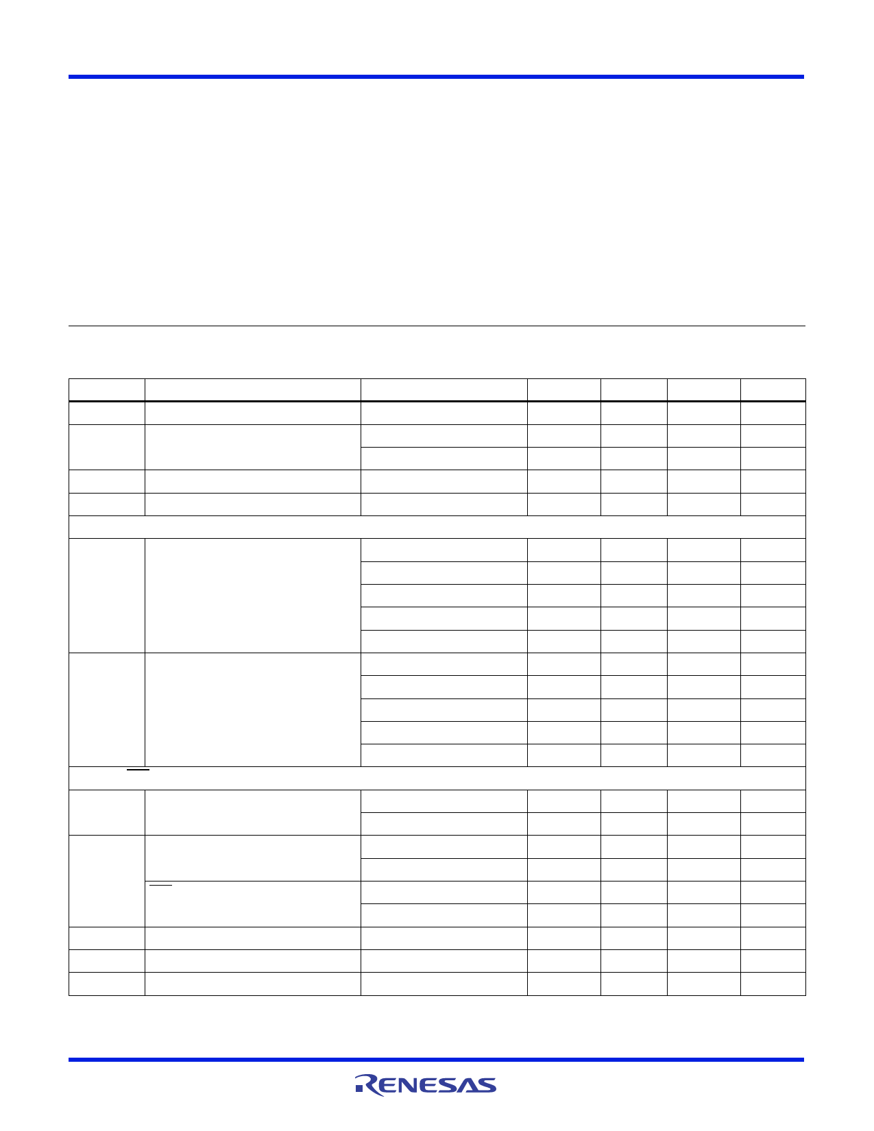
Electrical Specifications
Over the recommended operating conditions unless otherwise specified. Parameters with MIN and/or MAX
limits are 100% tested at +25В°C, unless otherwise specified. Temperature limits established by characterization
and are not production tested.
SYMBOL
PARAMETER
CONDITIONS
MIN
TYP
MAX
UNITS
VDD
IDD
Supply Voltage Range
ILI
Input Leakage Current (PFI)
ILO
Output Leakage Current
VOLTAGE THRESHOLDS
VDD = 5V, WDT Inactive
VDD = 3V, WDT Inactive
2.0
5.5
V
10
19
ВөA
8
10
ВөA
100
nA
100
nA
VTH1
Fixed VDD Voltage Trip Point
4.556
4.640
4.724
V
4.301
4.380
4.459
V
3.034
3.090
3.146
V
2.867
2.920
2.973
V
2.583
2.630
2.677
V
VTH1HYST Hysteresis at VTH1 Input
Temperature = +25В°C
RST AND RST
VTH1 = 4.64V
VTH1 = 4.38V
VTH1 = 3.09V
VTH1 = 2.92V
VTH1 = 2.63V
46
mV
44
mV
37
mV
29
mV
31
mV
VOL
Reset Output Voltage Low
VDD пӮі 3.3V, Sinking 2.5mA
0.05
0.40
V
VDD < 3.3V, Sinking 1.5mA
0.05
0.40
V
VOH
RST Output Voltage High
VDD пӮі 3.3V, Sourcing 2.5mA
VDD - 0.6 VDD - 0.4
V
VDD < 3.3V, Sourcing 1.5mA
VDD - 0.6 VDD - 0.4
V
RST Output Voltage High
VDD пӮі 3.3V, Sourcing 0.8mA
VDD - 0.6 VDD - 0.4
V
VDD < 3.3V, Sourcing 0.5mA
VDD - 0.6 VDD - 0.4
V
tRPD
VTH to Reset Asserted Delay
45
Вөs
tPOR
POR Time-Out Delay
CPOR is open
140
200
260
ms
CLOAD Load Capacitance on Reset Pins
5
pF
FN8092 Rev 6.00
November 30, 2015
Page 5 of 16
Share Link: