IRS25091SPBF データシートの表示(PDF) - International Rectifier
部品番号
コンポーネント説明
メーカー
IRS25091SPBF Datasheet PDF : 21 Pages
| |||
IRS25091SPbF
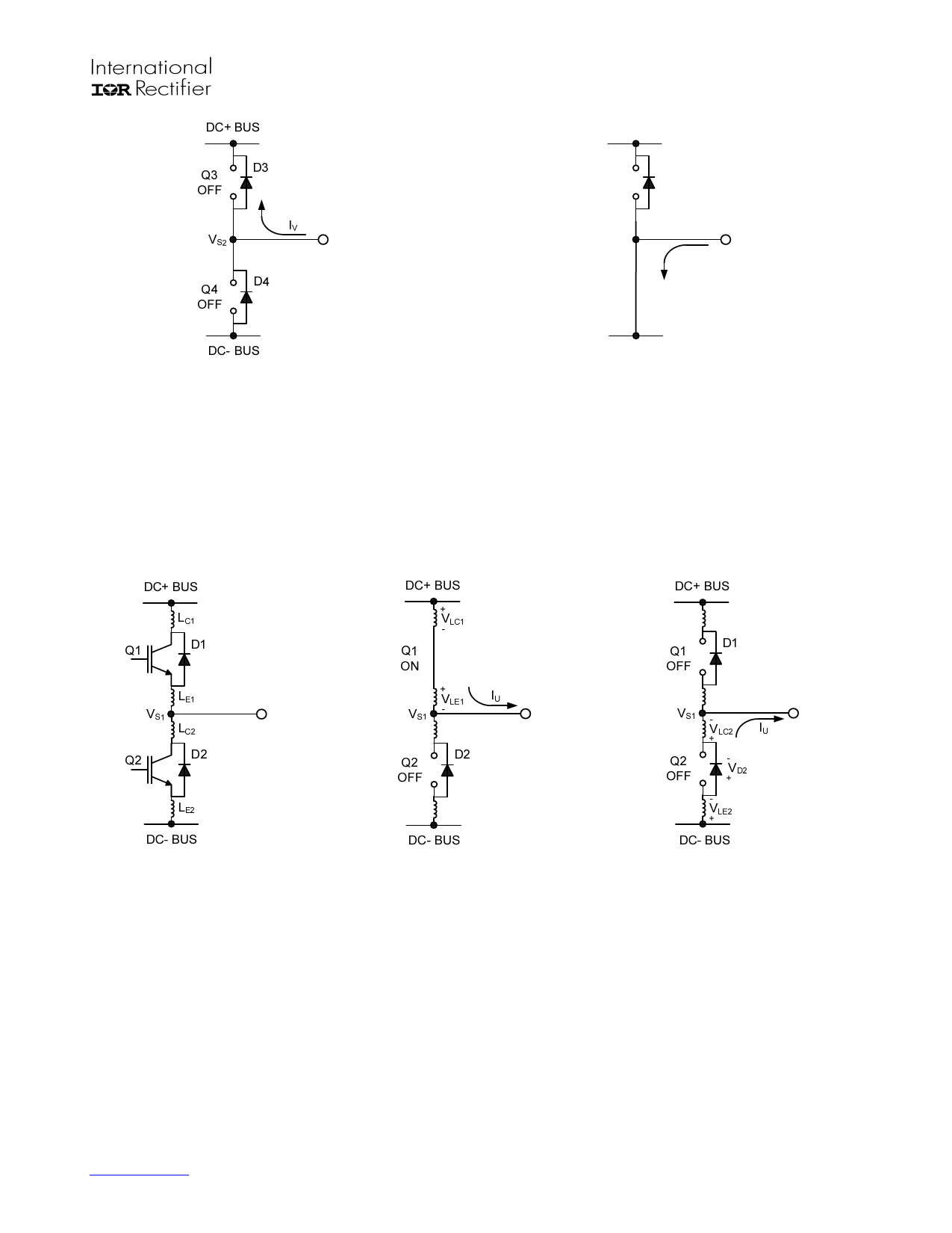
DC+ BUS
Q3
D3
OFF
VS2
IV
Q4
ON
Figure 14: D3 conducting
DC- BUS
Figure 15: Q4 conducting
However, in a real inverter circuit, the VS voltage swing does not stop at the level of the negative DC bus, rather it swings below the
level of the negative DC bus. This undershoot voltage is called “negative VS transient”.
The circuit shown in Figure 16 depicts one leg of the three phase inverter; Figures 17 and 18 show a simplified illustration of the
commutation of the current between Q1 and D2. The parasitic inductances in the power circuit from the die bonding to the PCB tracks
are lumped together in LC and LE for each IGBT. When the high-side switch is on, VS1 is below the DC+ voltage by the voltage drops
associated with the power switch and the parasitic elements of the circuit. When the high-side power switch turns off, the load current
momentarily flows in the low-side freewheeling diode due to the inductive load connected to VS1 (the load is not shown in these
figures). This current flows from the DC- bus (which is connected to the COM pin of the HVIC) to the load and a negative voltage
between VS1 and the DC- Bus is induced (i.e., the COM pin of the HVIC is at a higher potential than the VS pin).
Figure 16: Parasitic Elements
Figure 17: VS positive
Figure 18: VS negative
In a typical motor drive system, dV/dt is typically designed to be in the range of 3-5 V/ns. The negative VS transient voltage can
exceed this range during some events such as short circuit and over-current shutdown, when di/dt is greater than in normal operation.
International Rectifier’s HVICs have been designed for the robustness required in many of today’s demanding applications. An
indication of the IRS25091’s robustness can be seen in Figure 19, where there is represented the IRS25091 Safe Operating Area at
VBS=15V based on repetitive negative VS spikes. A negative VS transient voltage falling in the grey area (outside SOA) may lead to IC
permanent damage; viceversa unwanted functional anomalies or permanent damage to the IC do not appear if negative Vs transients
fall inside SOA.
At VBS=15V in case of -VS transients greater than -16.5 V for a period of time greater than 50 ns; the HVIC will hold by design the
high-side outputs in the off state for 4.5 μs.
www.irf.com
11
Share Link: 