IRS25091SPBF データシートの表示(PDF) - International Rectifier
部品番号
コンポーネント説明
メーカー
IRS25091SPBF Datasheet PDF : 21 Pages
| |||
IRS25091SPbF
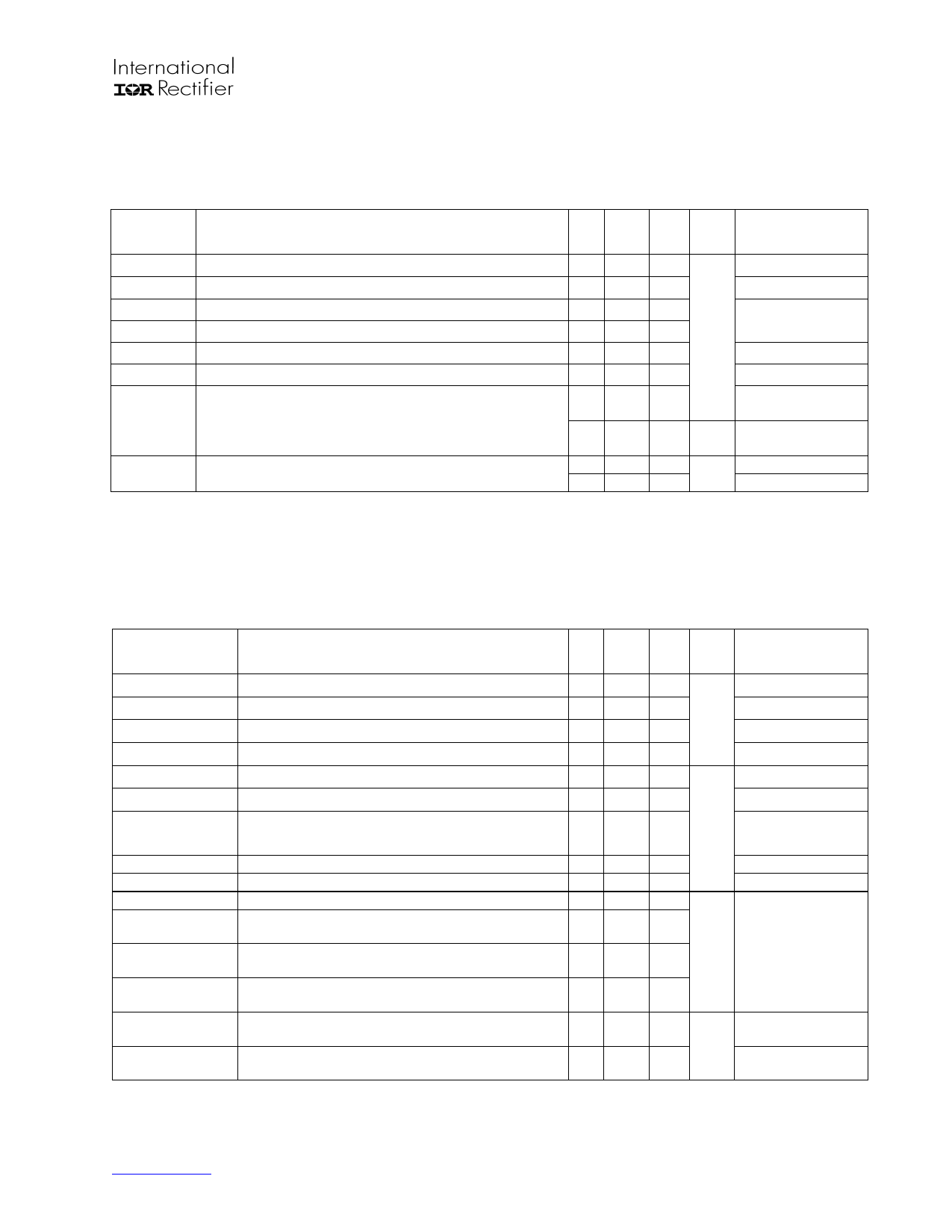
Dynamic Electrical Characteristics
VBIAS (VCC, VBS) = 15 V, COM = VCC, CL = 1000 pF, TA = 25 °C, DT = VSS unless otherwise specified.
Symbol
ton
toff
tsd
MT
tr
tf
DT
MDT
Definition
Turn-on propagation delay
Turn-off propagation delay
Shut-down propagation delay
Delay matching, HS & LS turn-on/off
Turn-on rise time
Turn-off fall time
Deadtime: LO turn-off to HO turn-on(DTLO-HO) &
HO turn-off to LO turn-on (DTHO-LO)
Deadtime matching = DTLO-HO - DTHO-LO
Min Typ Max Units Test Conditions
— 750 1100
— 250 400
— 250 400
— — 60 ns
— 150 220
— 50 80
VS = 0 V or 600 V
VS = 0 V or 600 V
VS = 0 V
VS = 0 V
350 530 800
RDT = 0 ohms
3 4.5 6 us RDT = 200K ohms
—
—
—
—
60
1100
ns
RDT = 0 ohms
RDT = 200K ohms
Static Electrical Characteristics
VBIAS (VCC, VBS) = 15 V, VCC = COM and TA = 25 °C unless otherwise specified. The VIL, VIH and IIN parameters are
referenced to VCC/COM and are applicable to the respective input leads: IN and DT/SD. The VO, IO parameters are
referenced to COM and are applicable to the respective output leads: HO and LO.
Symbol
VIH
VIL
VOH
VOL
ILK
IQBS
IQCC
IIN+
IIN-
ISD, TH
VCCUV+
VBSUV+
VCCUV-
VBSUV-
VCCUVH
VBSUVH
IO+
IO-
Definition
logic “1” input voltage for HO & logic “0” for LO
logic “0” input voltage for HO & logic “1” for LO
High level output voltage, VBIAS - VO
Low level output voltage, VO
Offset supply leakage current
Quiescent VBS supply current
Quiescent VCC supply current
Min Typ Max Units Test Conditions
2.2 — —
— — 0.8 V
— 0.8 1.4
— 0.3 0.6
— — 50
— 45 70
IO = 20 mA
IO = 20 mA
VB = VS = 600 V
VIN = 0 V or 4 V
1000 2000 3000 µA
VIN = 0 V or 4 V
Logic “1” input bias current
— 5 20
Logic “0” input bias current
—— 2
DT/SD input threshold
11.5 13 14.5
VCC and VBS supply undervoltage positive going
Threshold
8.0
8.9
9.8
VCC and VBS supply undervoltage negative going
Threshold
7.4
8.2
9.0
V
Hysteresis
— 0.7 —
Output high short circuit pulsed current
Output low short circuit pulsed current
120 200 —
mA
250 350 —
VIN = 4 V
VIN = 0 V
VO = 0 V,
PW ≤ 10 us
VO = 15 V,
PW ≤ 10 us
www.irf.com
4
Share Link: 