BD12734F データシートの表示(PDF) - ROHM Semiconductor
部品番号
コンポーネント説明
メーカー
BD12734F Datasheet PDF : 54 Pages
| |||
BD12730G BD12732xxx BD12734xxx
Datasheet
Line-up
Operating
Temperature
-40°C to +85°C
Channels
1ch
2ch
4ch
Package
SSOP5
SOP8
SOP-J8
SSOP-B8
TSSOP-B8
MSOP8
TSSOP-B8J
SOP14
SOP-J14
SSOP-B14
TSSOP-B14J
Reel of 3000
Reel of 2500
Reel of 2500
Reel of 2500
Reel of 3000
Reel of 3000
Reel of 2500
Reel of 2500
Reel of 2500
Reel of 2500
Reel of 2500
Orderable Part Number
BD12730G-TR
BD12732F-E2
BD12732FJ-E2
BD12732FV-E2
BD12732FVT-E2
BD12732FVM-TR
BD12732FVJ-E2
BD12734F-E2
BD12734FJ-E2
BD12734FV-E2
BD12734FVJ-E2
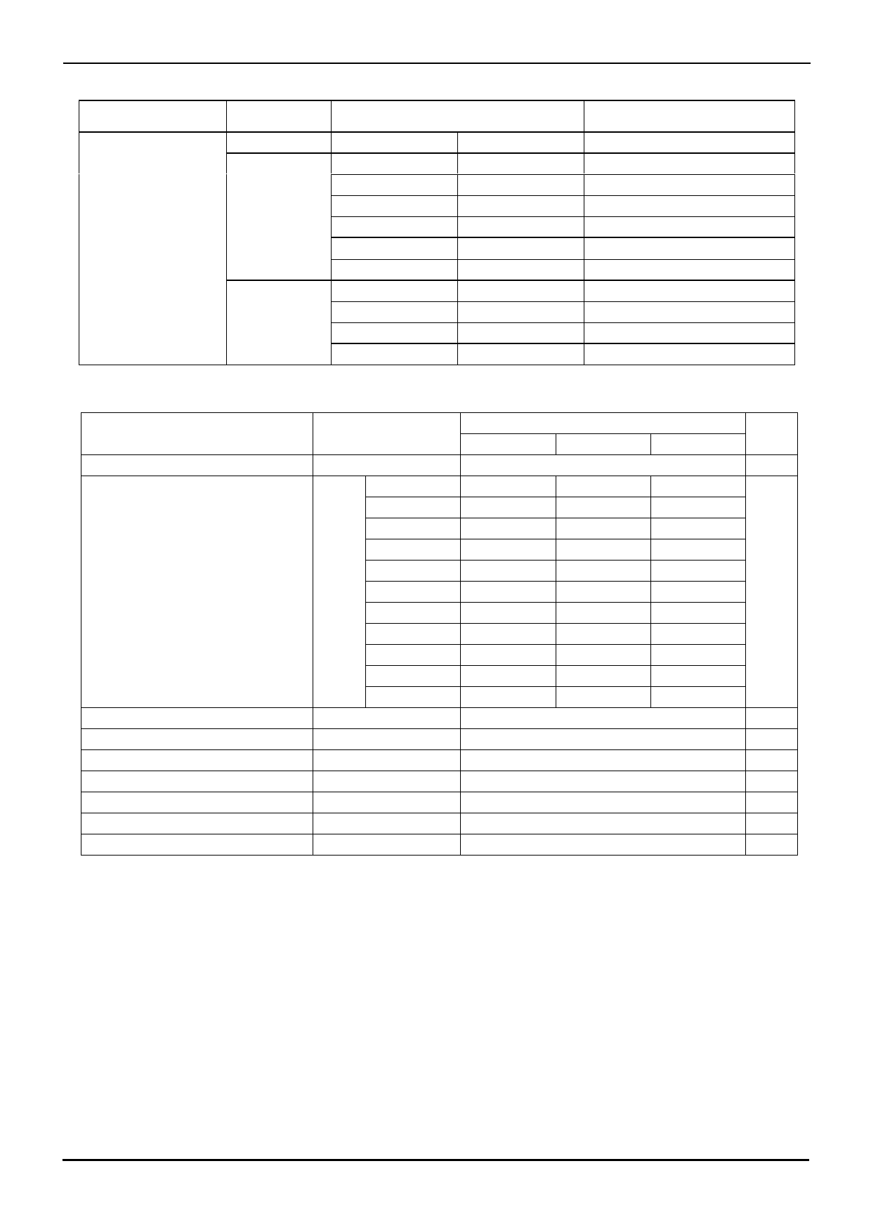
Absolute Maximum Ratings (TA=25°C)
Parameter
Symbol
BD12730G
Rating
BD12732xxx BD12734xxx
Unit
Supply Voltage
V+
+7.0
V
SSOP5
0.67 (Note 1,9)
-
-
SOP8
-
0.68 (Note 2,9)
-
SOP-J8
-
0.67 (Note 1,9)
-
SSOP-B8
-
0.62 (Note 3,9)
-
TSSOP-B8
-
0.62 (Note 3,9)
-
Power Dissipation
PD
MSOP8
-
0.58 (Note 4,9)
-
W
TSSOP-B8J
-
0.58 (Note 4,9)
-
SOP14
-
-
0.56(Note 5,9)
SOP-J14
-
-
1.02(Note 6,9)
SSOP-B14
-
-
0.87(Note 7,9)
TSSOP-B14J
-
-
0.85(Note 8,9)
Differential Input Voltage (Note 10)
VID
±3.0
V
Input Common-mode Voltage Range
VICM
GND to V+
V
Input Current (Note 11)
II
±10
mA
Operating Supply Voltage
Vopr
+1.8 to +5.5
V
Operating Temperature
Topr
- 40 to +85
°C
Storage Temperature
Tstg
- 55 to +150
°C
Maximum Junction Temperature
TJmax
+150
°C
(Note 1) To use at temperature above TA=25°C, reduce by 5.4mW/°C.
(Note 2) To use at temperature above TA=25°C, reduce by 5.5mW/°C.
(Note 3) To use at temperature above TA=25°C, reduce by 5.0mW/°C.
(Note 4) To use at temperature above TA=25°C, reduce by 4.7mW/°C.
(Note 5) To use at temperature above TA=25°C, reduce by 4.5mW/°C.
(Note 6) To use at temperature above TA=25°C, reduce by 8.2mW/°C.
(Note 7) To use at temperature above TA=25°C, reduce by 7.0mW/°C.
(Note 8) To use at temperature above TA=25°C, reduce by 6.8mW/°C.
(Note 9) Mounted on a FR4 glass epoxy PCB 70mm×70mm×1.6mm (Copper foil area less than 3%).
(Note 10) Differential Input Voltage is the voltage difference between the inverting and non-inverting inputs.
The input pin voltage is set to more than GND.
(Note 11) An excessive input current will flow when input voltages of more than Supply Voltage(V+)+0.6V or less than GND-0.6V are applied.
The input current can be set to less than the rated current by adding a limiting resistor.
Caution: Operating the IC over the absolute maximum ratings may damage the IC. The damage can either be a short circuit between pins or an open
circuit between pins and the internal circuitry. Therefore, it is important to consider circuit protection measures, such as adding a fuse, in case the
IC is operated over the absolute maximum ratings.
www.rohm.com
©2013 ROHM Co., Ltd. All rights reserved.
TSZ22111・15・001
3/50
TSZ02201-0GMG0G200600-1-2
14.July.2016.Rev004
Share Link: 