AD7522J データシートの表示(PDF) - Analog Devices
部品番号
コンポーネント説明
メーカー
AD7522J Datasheet PDF : 6 Pages
| |||
PIN FUNCTION DESCRIPTION
PIN MNEMONIC
1 VDD
2 LDTR
3 VREF
4 RFB2
5 RFBI
6 IoUTl
7 IoUTZ
8 AGND
+15V (nominal) Main Supply.
DESCRIPTION
R-2R Ladder Termination Resistor. Normally grounded for unipolar operation or terminated at 'oUT2 for bipolar operation.
Reference Voltage Input. Since the AD7522 is a multiplying DAC, VREF may vary over the range of :!:10V.
RFEEDBACK 7 2; gives full scale equal to VREF/2.
RFEEDBACK' used for normal unity gain (at full scale) D/A conversion.
DAC Current OUTI Bus. Normally terminated at virtUal ground of output amplifier.
DAC Current OUT2 Bus, terminated at ground for unipolar operation, or virtual ground of op amp for bipolar operation.
Analog Ground. Back gate of DAC N-channel SPOT current steering switches.
9 SRO
Serial Output. An auxiliary output for recovering data in the input buffer.
10
Data Bit 9. Most significant parallel data input.
11 DB8
Data Bit 8.
12 DB7
Data Bit 7.
13 DB6
Data Bit 6.
14 089T
Data Bit 5.
DB5 Note 1
15
Data Bit 4.
OBSOLETE 16 DB3
17 DB2
18 DBI
19 DMBOl
20 SC8
21 SPC
22 LDAC
23 NC
24 LBS
Data Bit 3.
Data Bit 2.
Data Bit 1.
Data Bit O. Least significant parallel data input.
8-Bit Short Cycle Control. When in serial mode, if scs is held to Logic "0", the two least significant input latches in the input buffer
are bypassed to provide proper serial loading of 8-bit serial words. If SC8 is held to Logic "1", the AD7522 will accept a to-bit serial
word.
-
= Data bits 0 (LSB) and DBI are in a parallel load mode when SC8 0 and should be tied to a logic low state to prevent fal~ data
from being loaded.
SeriallParalleI Control. If SPC is a Logic "0", the AD7522 will load parallel data appearing on DBO through DB9 into the input buffer
when the appropriate strobe inputs are exercised (see HBS and LBS).
If SPC is a Logic "1", the AD7522 will load serial data appearing on Pin 26 into the input buffers. Each serial data bit must be
"suobed" into the buffer with the HBS and LBS.
Load DAC: When LDAC is a Logic "0", the AD7522 is in the "hold" mode, and digital activity in the input buffer is locked out.
When LDAC is a Logic "I ", the AD7522 is in the "load" mode, and data in the input buffer loads the DAC register.
No Connection.
Low Byte Strobe. When in "parallel load" mode (SPC = 0), parallel data appearing on the DBO (LSB) through DB7 inputs will be
"clocked" into the input buffer on the positive going edge of the LBS.
When in "serial load" mode (SPC = 1), serial data bits appearing at the serial input terminal, Pin 26, will be "clocked" into the input
buffer on the positive going edge of HBS and LBS. (HBS and LBS must be clocked simultaneously when in "serial load" mode.)
25 HBS
High Byte Strobe. When in "parallel load" mode (SPC = 0), parallel data appearing on the DB9 (MSB) and DB8 data inputs will be
"clocked" into the input buffer on the positive going edge of HBS.
26 SRI
27 VCC
28 DGND
When in "serial load" mode (SPC = I), serial data bits appearing at the serial input terminal, Pin 26, will be "clocked" into the input
buffer on the positive going edges of HBS and LBS. (HBS and LBS muSt be clocked simultaneously when in "serial load" mode.)
Serial Input.
Logic Supply. If +5V is applied, all digital inputs/outputs are TTL compatible. If +10V to +15V is applied, digital inputs/outputs
are CMOS compatible.
Digital Ground
Note I, Logie "I" applied to a data bit steers that bit's cun-ent to the 10UTI tenninaJ.
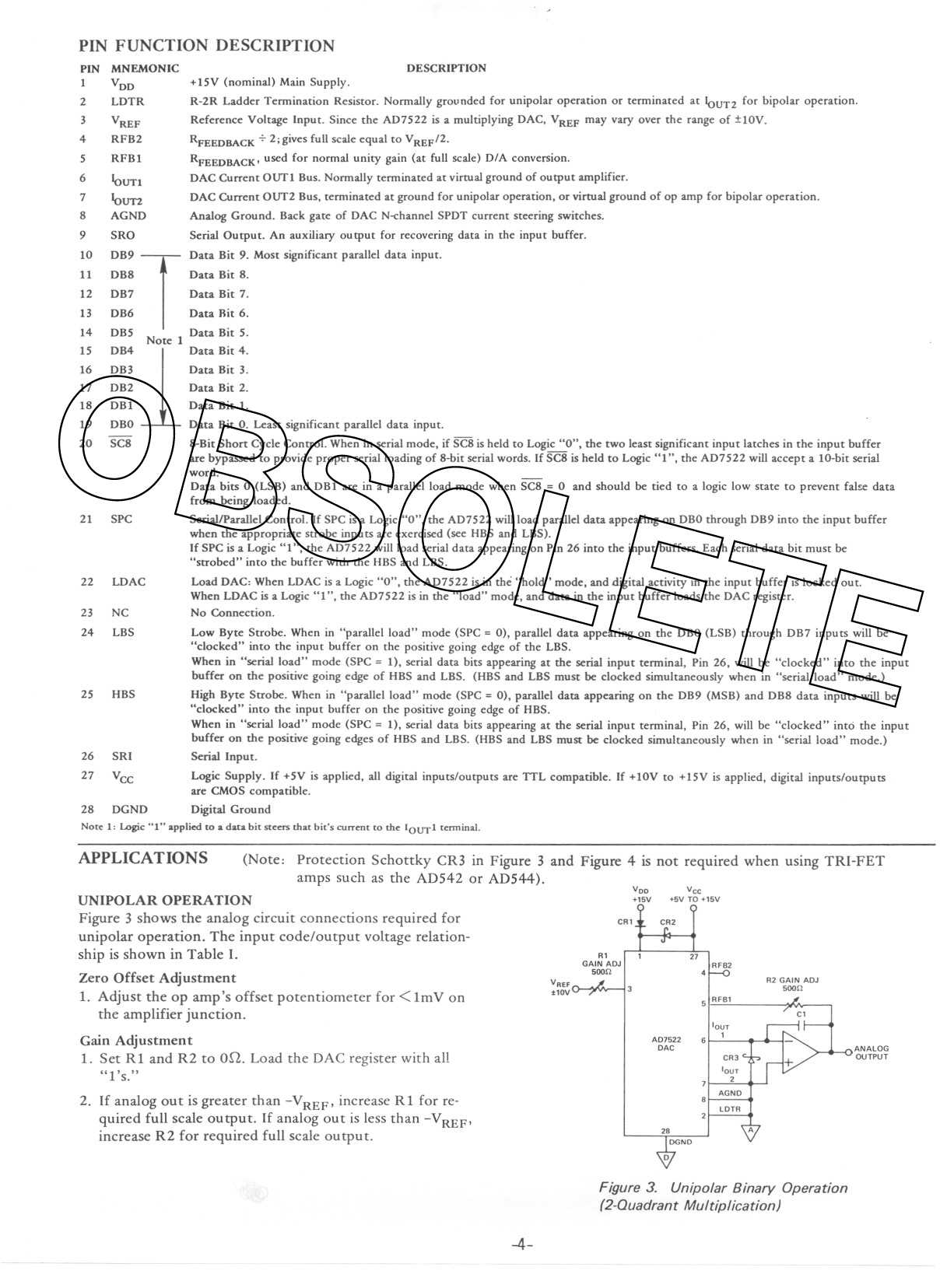
APPLICATIONS
(Note:
UNIPOLAR OPERATION
Protection Schottky CR3 in Figure 3 and Figure 4 is not required when using TRI-FET
amps such as the AD542 or AD544).
VDD
+15V
Vcc
+5V TO +15V
Figure 3 shows the analog circuit connections required for
CAI
unipolar operation. The input code/output voltage relation-
ship is shown in Table I.
Zero Offset Adjustment
1. Adjust the op amp's offset potentiometer for < 1mV on
the amplifier junction.
Gain Adjustment
1. Set Rl and R2 to oQ. Load the DAC register with all
"l's."
VREF
>IOY
AI
GAIN ADJ
5OOQ
27
AF82
4-
AD7522
DAC
5,AF81
'OUT
1
CA3
lOUT
2
A2 GAIN ADJ
500Q
ANALOG
OUTPUT
2, If analog out is greater than -VREF' increase Rl for re-
quired full scale output, If analog out is less than -VREF'
increase R2 for required full scale output.
LOTA
Figure 3. Unipolar Binary Operation
(2-Quadrant Multiplication)
-4-
Share Link: 