CY62128EV30LL-55ZXE データシートの表示(PDF) - Cypress Semiconductor
部品番号
コンポーネント説明
メーカー
CY62128EV30LL-55ZXE Datasheet PDF : 12 Pages
| |||
CY62128EV30 MoBL®
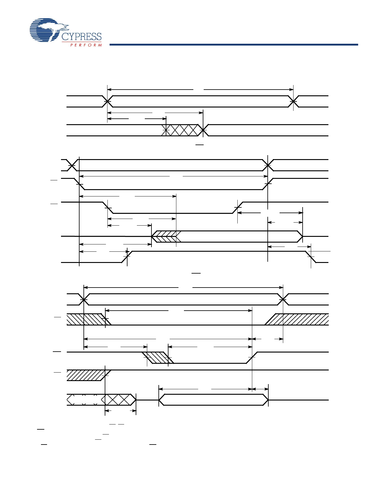
Switching Waveforms
Figure 6. Read Cycle 1 (Address transition controlled) [15, 16]
tRRCC
ADDRESS
DATA OUT
tAA
tOHA
PREVIOUS DATA VALID
DATA VALID
Figure 7. Read Cycle No. 2 (OE controlled) [10, 16, 17]
ADDRESS
CE
OE
DATA OUT
VCC
SUPPLY
CURRENT
ADDRESS
CE
tRC
tACE
tDOE
tLZOE
HIGH IMPEDANCE
tLZCE
tPU
50%
DATA VALID
tHZOE
tHZCE
HIGH
IMPEDANCE
tPD
ICC
50%
ISB
Figure 8. Write Cycle No. 1 (WE controlled) [10, 15, 18, 19]
tWC
tSCE
tAW
tHA
tSA
tPWE
WE
OE
tSD
tHD
DATA I/O
NOTE 20
DATA VALID
tHZOE
Notes
15. The device is continuously selected. OE, CE1 = VIL, CE2 = VIH.
16. WE is HIGH for read cycle.
17. Address valid before or similar to CE1 transition LOW and CE2 transition HIGH.
18. Data I/O is high impedance if OE = VIH.
19. If CE1 goes HIGH or CE2 goes LOW simultaneously with WE HIGH, the output remains in high impedance state.
20. During this period, the IOs are in output state. Do not apply input signals.
Document #: 38-05579 Rev. *E
Page 6 of 12
[+] Feedback
Share Link: 