Q68000A8640 гғҮгғјгӮҝгӮ·гғјгғҲгҒ®иЎЁзӨәпјҲPDFпјү - OSRAM GmbH
йғЁе“Ғз•ӘеҸ·
гӮігғігғқгғјгғҚгғігғҲиӘ¬жҳҺ
гғЎгғјгӮ«гғј
Q68000A8640 Datasheet PDF : 10 Pages
| |||
SLR2016, SLO2016, SLG2016, SLY2016, SCD5584A
Pin Function
Pin
Function
1
WR Write
2
A1 Digit Select
3
A0 Digit Select
4
VCC
Pin
Function
8
D3 Data
9
D4 Data
10
D5 Data
11
D6 Data
Pin Function
Pin
Function
5
D0 Data
6
D1 Data
7
D2 Data
Pin
Function
12
BL Display Blank
13
CLR Clear
14
GND
DC Characteristics at 25В°C
Parameters
VCC
ICC Blank
ICC (80 dots on)
VIL (all inputs)
VIH (all inputs)
IIL (all inputs)
Min.
4.5
вҖ”
вҖ”
вҖ”
2.0
25
Typ.
5.0
2.3
80
вҖ”
вҖ”
вҖ”
AC Characteristics (guaranteed minimum timing
parameters at VCC=5.0 V Вұ0.5 V)
Parameter
Symbol вҖ“40В°C +25В°C +85В°C Unit
Address Set TAS
Up Time
10
10
10
ns
Write Time
TW
Data Set Up TDS
Time
60
70
90
ns
20
30
50
ns
Address Hold TAH
Time
20
30
40
ns
Data Hold
TDH
Time
20
30
40
ns
Access Time TACC (1)
90
Clear Disable TCLRD
1.0
Time
110
140
ns
1.0
1.0
Вөs
Clear Time
TCLR
1.0
1.0
1.0
ms
Note:
1) TACC=Set Up Time + Write Time + Hold Time
Max.
5.5
3.0
105
0.8
вҖ”
100
Units
V
mA
mA
V
V
ВөA
Conditions
вҖ”
VCC=5.0 V
VCC=5.0 V
4.5 V <VCC <5.5 V
4.5 V <VCC <5.5 V
4.5 V <VCC <5.5 V, VIN=0.8 V
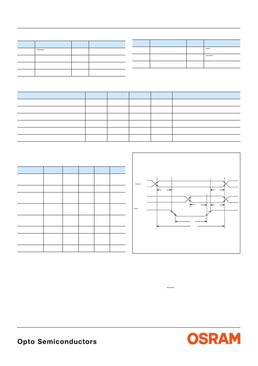
Timing CharacteristicsвҖ”Write Cycle Waveforms
A0 вҖ“ A1
CLR
TAS
D0 вҖ“ D6
WR
TDS
TW
TACC
2.0 V
0.8 V
TAH
2.0 V
0.8 V
TDH
2.0 V
0.8 V
Loading Data
The desired data code (D0вҖ“D6) and digit address (A0, A1) must
be held stable during the write cycle for storing new data.
Data entry may be asynchronous. Digit 0 is defined as right hand
digit with A1=A2=0.
Clearing the entire internal four-digit memory can be accomplished
by holding the clear (CLR) low for 1.0 msec minimum. The clear
function will clear the ASCII RAM. Loading an illegal data code will
display a blank.
2006-01-23
4
Share Link: 