ES3JF(2019) データシートの表示(PDF) - Jiangsu Yutai Electronics Co., Ltd
部品番号
コンポーネント説明
メーカー
ES3JF Datasheet PDF : 3 Pages
| |||
ES3AF THRU ES3JF
Reverse Voltage - 50 to 600 Volts Forward Current - 3.0 Ampere
SURFACE MOUNT SUPER FAST RECOVERY RECTIFIER
Features
The plastic package carries Underwriters Laboratory
Flammability Classification 94V-0
For surface mounted applications
Low reverse leakage
Built-in strain relief,ideal for automated
placement High forward surge current capability
High temperature soldering guaranteed:
250°C/10 seconds at terminals
Glass passivated chip junction
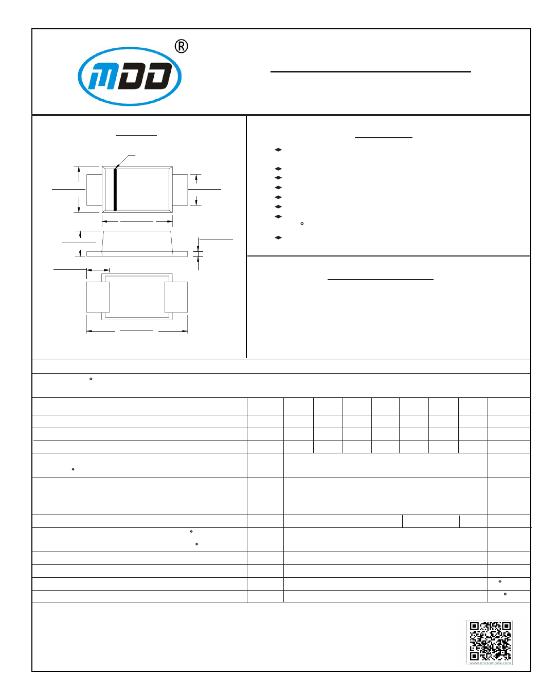
Mechanical Data
Case : JEDEC SMAF Molded plastic body
Terminals : Solder plated, solderable per MIL-STD-750,Method 2026
Polarity : Polarity symbol marking on body
Mounting Position : Any
Weight : 0.00095 ounce, 0.027 grams
0.063 (1.60)
0.051 (1.30)
SMAF
0.146(3.70)
0.130(3.30)
0.106(2.70)
0.094(2.40)
0.047(1.20)
0.035(0.90)
0.047(1.20)
0.031(0.80)
0.193(4.90)
0.173(4.40)
0.008(0.20)
0.005(0.12)
Dimensions in inches and (millimeters)
Maximum Ratings And Electrical Characteristics
Ratings at 25 C ambient temperature unless otherwise specified.
Single phase half-wave 60Hz,resistive or inductive load,for capacitive load current derate by 20%.
Parameter
Marking Code
Maximum repetitive peak reverse voltage
Maximum RMS voltage
Maximum DC blocking voltage
Maximum average forward rectified current
at TL=55℃
ES3AF
SYMBOLS MDD
ES3AF
VRMM
50
VRMS
35
VDC
50
I(AV)
ES3BF
MDD
ES3BF
100
70
100
ES3CF
MDD
ES3CF
150
105
150
ES3DF
MDD
ES3DF
200
140
200
3.0
ES3EF
MDD
ES3EF
300
210
300
ES3GF
MDD
ES3GF
400
280
400
ES3JF
MDD
ES3JF
600
420
600
Peak forward surge current
8.3ms single half sine-wave
superimposed onrated load (JEDEC Method)
IFSM
80
UNITS
V
V
V
A
A
Maximum instantaneous forward voltage at 3.0A
Maximum DC reverse current
at rated DCblocking voltage
TA=25℃
TA=125℃
Maximum reverse recovery time (NOTE 1)
Typical junction capacitance (NOTE 2)
Typical thermal resistance (NOTE 3)
Operating junction and storage temperature range
VF
IR
trr
CJ
RJA
TJ,TSTG
1
1.25
5.0
100.0
35
40.0
50.0
-55 to +150
Note:1.Reverse recovery condition IF=0.5A,IR=1.0A,Irr=0.25A
2.P.C.B. mounted with 2.0" X 2.0" (5 X 5 cm) copper pad areas.
3.Measured at 1MHz and applied reverse voltage of 4.0V D.C.
4.The typical data above is for referenceonly.
1.68
V
μA
ns
pF
℃/W
℃
DN:T19712A0
https://www.microdiode.com
Rev:2019A0
Page :1
Share Link: 