MMFT1N10E データシートの表示(PDF) - Motorola => Freescale
部品番号
コンポーネント説明
メーカー
MMFT1N10E Datasheet PDF : 10 Pages
| |||

MMFT1N10E
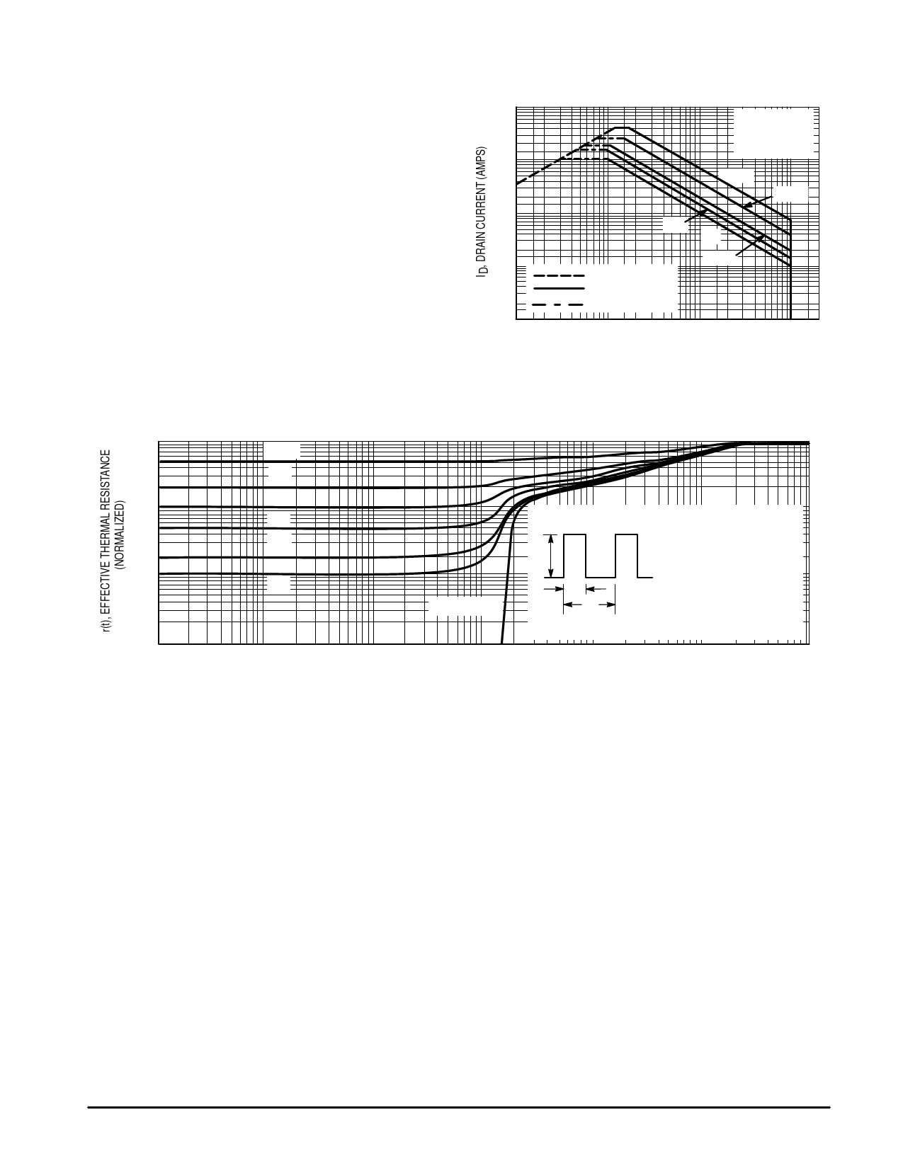
FORWARD BIASED SAFE OPERATING AREA
The FBSOA curves define the maximum drain–to–source
voltage and drain current that a device can safely handle
when it is forward biased, or when it is on, or being turned on.
Because these curves include the limitations of simultaneous
high voltage and high current, up to the rating of the device,
they are especially useful to designers of linear systems. The
curves are based on an ambient temperature of 25°C and a
maximum junction temperature of 150°C. Limitations for re-
petitive pulses at various ambient temperatures can be de-
termined by using the thermal response curves. Motorola
Application Note, AN569, “Transient Thermal Resistance–
General Data and Its Use” provides detailed instructions.
SWITCHING SAFE OPERATING AREA
The switching safe operating area (SOA) is the boundary
that the load line may traverse without incurring damage to
the MOSFET. The fundamental limits are the peak current,
IDM and the breakdown voltage, BVDSS. The switching SOA
is applicable for both turn–on and turn–off of the devices for
switching times less than one microsecond.
10
1
0.1
0.01
0.001
0.1
VGS = 20 V
SINGLE PULSE
TA = 25°C
20 ms
100 ms
1s
RDS(on) LIMIT
THERMAL LIMIT
PACKAGE LIMIT
DC
500 ms
1
10
100
VDS, DRAIN–TO–SOURCE VOLTAGE (VOLTS)
Figure 7. Maximum Rated Forward Biased
Safe Operating Area
1.0
0.1
0.01
0.001
1.0E–05
D = 0.5
0.2
0.1
0.05
0.02
0.01
1.0E–04
1.0E–03
SINGLE PULSE
1.0E–02
t, TIME (s)
P(pk)
t1
t2
RθJA(t) = r(t) RθJA
RθJA = 156°C/W MAX
D CURVES APPLY FOR POWER
PULSE TRAIN SHOWN
READ TIME AT t1
TJ(pk) – TA = P(pk) RθJA(t)
DUTY CYCLE, D = t1/t2
1.0E–01
1.0E+00
1.0E+01
Figure 8. Thermal Response
COMMUTATING SAFE OPERATING AREA (CSOA)
The Commutating Safe Operating Area (CSOA) of Figure 10 defines the limits of safe operation for commutated source–drain
current versus re–applied drain voltage when the source–drain diode has undergone forward bias. The curve shows the limita-
tions of IFM and peak VDS for a given rate of change of source current. It is applicable when waveforms similar to those of Figure
9 are present. Full or half–bridge PWM DC motor controllers are common applications requiring CSOA data.
Device stresses increase with increasing rate of change of source current so dIS/dt is specified with a maximum value. Higher
values of dIS/dt require an appropriate derating of IFM, peak VDS or both. Ultimately dIS/dt is limited primarily by device, package,
and circuit impedances. Maximum device stress occurs during trr as the diode goes from conduction to reverse blocking.
VDS(pk) is the peak drain–to–source voltage that the device must sustain during commutation; IFM is the maximum forward
source–drain diode current just prior to the onset of commutation.
VR is specified at 80% rated BVDSS to ensure that the CSOA stress is maximized as IS decays from IRM to zero.
RGS should be minimized during commutation. TJ has only a second order effect on CSOA.
Stray inductances in Motorola’s test circuit are assumed to be practical minimums. dVDS/dt in excess of 10 V/ns was at-
tained with dIS/dt of 400 A/µs.
4
Motorola TMOS Power MOSFET Transistor Device Data