NCV8842PWGEVB データシートの表示(PDF) - ON Semiconductor
部品番号
コンポーネント説明
メーカー
NCV8842PWGEVB
ON Semiconductor

NCV8842PWGEVB Datasheet PDF : 11 Pages
| |||
NCV8842PWGEVB
SHUTDOWN
1 TP1
SYNC
1 TP2
Vout
BR3 BR2 BR1
D1 R5
0
C1
L1 1 mF
27 mH
D2
+
C3
100 mF
R4 R3 R1
374 205 124
R6
10k
U1
Vsw
SHDNB
NC
NC
NC
NC
SYNC
GND
Vin
BOOST
NC
NC
NC
NC
Vc
Vfb
NCV8842
R2
127
Vin
C4
C5
0.1 mF 0.1 mF
+ C2
330 mF
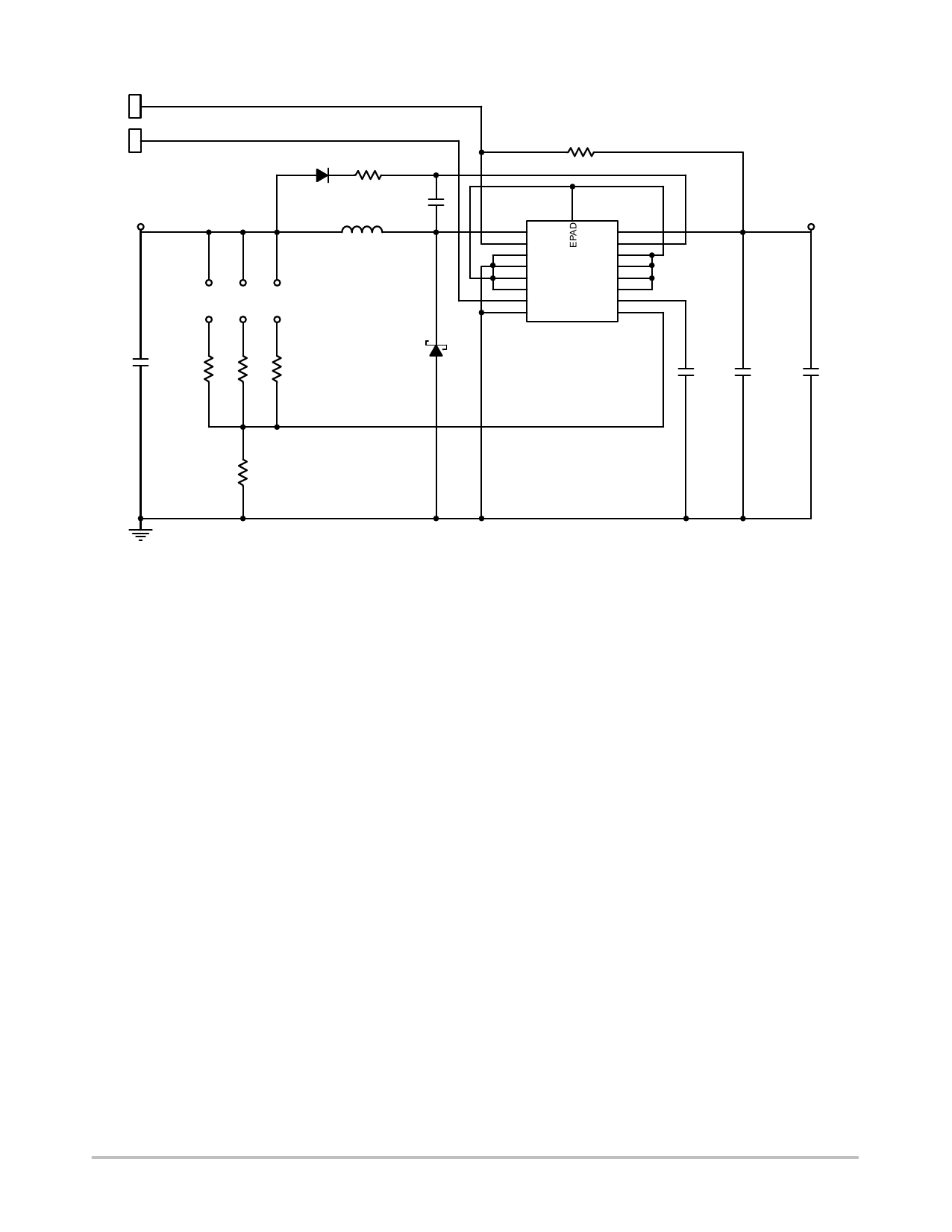
Figure 2. Application Diagram
Operation Guidelines
1. Connect a DC input voltage, within the range of 7.0 V
to 16 V, between the board terminals “VIN” (+) and
“GND” (−).
2. Connect a load impedance between terminals “VOUT”
(+) and “GND” (−).
3. To force the regulator into Shutdown/sleep mode,
connect the “SHDNB” terminal to a positive DC
voltage of 0.3 V or less, or connect it directly to GND.
4. If synchronization to an external frequency source is
desired, connect the SYNC terminal to a pulse source
with positive amplitude 1 V to 7 V relative to GND.
Sync pulse duty cycle may vary from 10% to 90%.
Theory Of Operation
1. Boost Circuit: The Boost circuit, comprised of D1 and
C1, generates a voltage higher than the output voltage
to drive the base of the internal NPN power switch.
When the internal power switch is Off, pin Vsw of the
NCV8842 goes negative to sustain the current in L1
through Schottky diode D2. Diode D1 is forward
biased, and charges C1 to approximately the output
voltage. When the internal power switch turns on, Vsw
is driven high, forcing the voltage at BOOST to be the
sum of the instantaneous voltage at Vsw plus the
charge across C1. D1 is now reverse−biased, and the
energy stored in C1 is used to bias the output stage.
2. Soft Start: The soft−start is implemented on the VC pin.
During the startup, the limited source current (25 μA)
of the error amplifier charges the VC pin capacitor. The
rising slope of the VC pin voltage clamps the duty cycle
through the PWM comparator. The VC pin voltage
eventually settles down to a voltage roughly equal to the
reference voltage 1.27 V. Therefore, the startup time can
be easily calculated.
3. Feedback Network: V2 control relies on the output
ripple to provide pulse width modulation. When the
output ripple is inadequate, pulse skipping or
instability may be observed. Adding a capacitor C6 in
parallel with R1 provides a low impedance pass for the
output ripple. Therefore, the output ripple is not
attenuated by the resistor divider. The use of this
capacitor is optional.
Please see data sheet for more description on regulator
operation and component selection (document number
NCV8842/D available through the Literature
Distribution Center or via our website at
http://www.onsemi.com).
http://onsemi.com
3
Share Link: