M24C01(2000) гғҮгғјгӮҝгӮ·гғјгғҲгҒ®иЎЁзӨәпјҲPDFпјү - STMicroelectronics
йғЁе“Ғз•ӘеҸ·
гӮігғігғқгғјгғҚгғігғҲиӘ¬жҳҺ
гғЎгғјгӮ«гғј
M24C01 Datasheet PDF : 20 Pages
| |||
M24C16, M24C08, M24C04, M24C02, M24C01
Table 3. Device Select Code 1
Device Type Identifier
Chip Enable
RW
b7
b6
b5
b4
b3
b2
b1
b0
M24C01 Select Code
1
0
1
0
E2
E1
E0
RW
M24C02 Select Code
1
0
1
0
E2
E1
E0
RW
M24C04 Select Code
1
0
1
0
E2
E1
A8
RW
M24C08 Select Code
1
0
1
0
E2
A9
A8
RW
M24C16 Select Code
1
0
1
0
A10
A9
Note: 1. The most significant bit, b7, is sent first.
2. E0, E1 and E2 are compared against the respective external pins on the memory device.
3. A10, A9 and A8 represent high significant bits of the address.
A8
RW
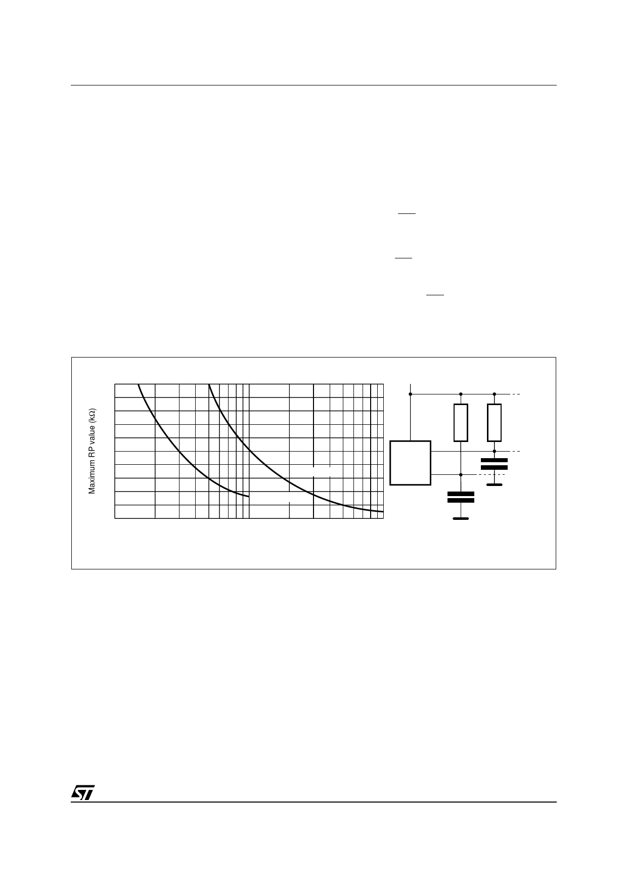
Write Control (WC)
The hardware Write Control pin (WC) is useful for
protecting the entire contents of the memory from
inadvertent erase/write. The Write Control signal is
used to enable (WC=VIL) or disable (WC=VIH)
write instructions to the entire memory area. When
unconnected, the WC input is internally read as
VIL, and write operations are allowed.
When WC=1, Device Select and Address bytes
are acknowledged, Data bytes are not
acknowledged.
Please see the Application Note AN404 for a more
detailed description of the Write Control feature.
DEVICE OPERATION
The memory device supports the I2C protocol.
This is summarized in Figure 4, and is compared
with other serial bus protocols in Application Note
AN1001. Any device that sends data on to the bus
is defined to be a transmitter, and any device that
reads the data to be a receiver. The device that
controls the data transfer is known as the master,
and the other as the slave. A data transfer can only
be initiated by the master, which will also provide
the serial clock for synchronization. The memory
device is always a slave device in all
communication.
Start Condition
START is identified by a high to low transition of
the SDA line while the clock, SCL, is stable in the
high state. A START condition must precede any
data transfer command. The memory device
continuously monitors (except during a
programming cycle) the SDA and SCL lines for a
START condition, and will not respond unless one
is given.
Stop Condition
STOP is identified by a low to high transition of the
SDA line while the clock SCL is stable in the high
state. A STOP condition terminates
communication between the memory device and
the bus master. A STOP condition at the end of a
Read command, after (and only after) a NoAck,
forces the memory device into its standby state. A
STOP condition at the end of a Write command
triggers the internal EEPROM write cycle.
Acknowledge Bit (ACK)
An acknowledge signal is used to indicate a
successful byte transfer. The bus transmitter,
whether it be master or slave, releases the SDA
bus after sending eight bits of data. During the 9th
Table 4. Operating Modes
Mode
RW bit
Current Address Read
1
0
Random Address Read
1
Sequential Read
1
Byte Write
0
Page Write
0
Note: 1. X = VIH or VIL.
WC 1
X
X
X
X
VIL
VIL
Bytes
1
1
вүҘ1
1
вүӨ 16
Initial Sequence
START, Device Select, RW = вҖҳ1вҖҷ
START, Device Select, RW = вҖҳ0вҖҷ, Address
reSTART, Device Select, RW = вҖҳ1вҖҷ
Similar to Current or Random Address Read
START, Device Select, RW = вҖҳ0вҖҷ
START, Device Select, RW = вҖҳ0вҖҷ
5/20
Share Link: 