M24C01(2000) гғҮгғјгӮҝгӮ·гғјгғҲгҒ®иЎЁзӨәпјҲPDFпјү - STMicroelectronics
йғЁе“Ғз•ӘеҸ·
гӮігғігғқгғјгғҚгғігғҲиӘ¬жҳҺ
гғЎгғјгӮ«гғј
M24C01 Datasheet PDF : 20 Pages
| |||
M24C16, M24C08, M24C04, M24C02, M24C01
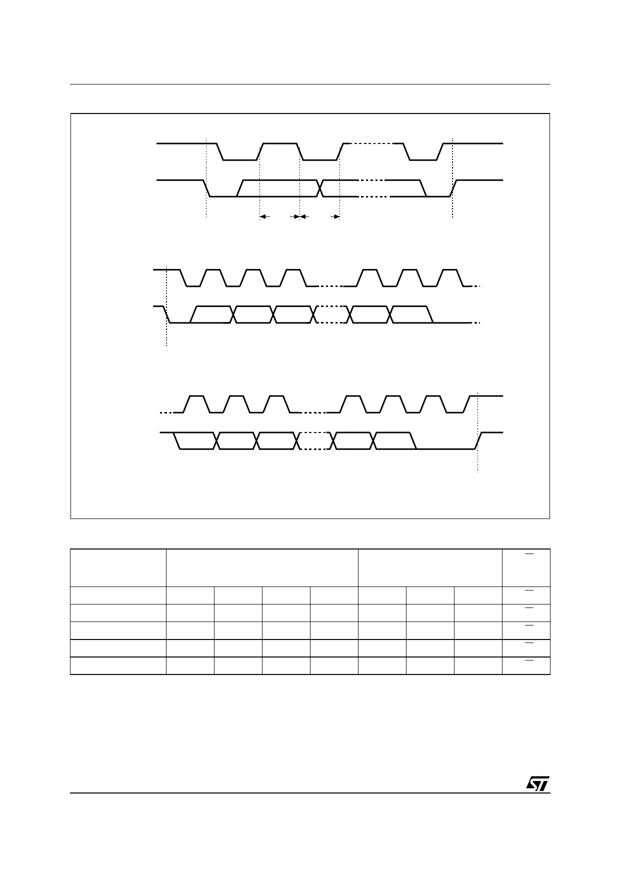
Figure 5. Write Mode Sequences with WC=1 (data write inhibited)
WC
BYTE WRITE
ACK
ACK
NO ACK
DEV SEL
BYTE ADDR
DATA IN
R/W
WC
PAGE WRITE
WC (cont'd)
PAGE WRITE
(cont'd)
ACK
ACK
NO ACK
NO ACK
DEV SEL
BYTE ADDR DATA IN 1
DATA IN 2
DATA IN 3
R/W
NO ACK
NO ACK
DATA IN N
AI02803B
clock pulse period, the receiver pulls the SDA bus
low to acknowledge the receipt of the eight data
bits.
Data Input
During data input, the memory device samples the
SDA bus signal on the rising edge of the clock,
SCL. For correct device operation, the SDA signal
must be stable during the clock low-to-high
transition, and the data must change only when
the SCL line is low.
Memory Addressing
To start communication between the bus master
and the slave memory, the master must initiate a
START condition. Following this, the master sends
the 8-bit byte, shown in Table 3, on the SDA bus
line (most significant bit first). This consists of the
7-bit Device Select Code, and the 1-bit Read/Write
Designator (RW). The Device Select Code is
further subdivided into: a 4-bit Device Type
Identifier, and a 3-bit Chip Enable вҖңAddressвҖқ (E2,
E1, E0).
To address the memory array, the 4-bit Device
Type Identifier is 1010b.
Up to eight memory devices can be connected on
a single I2C bus. Each one is given a unique 3-bit
code on its Chip Enable inputs. When the Device
Select Code is received, the memory only
responds if the Chip Enable Code (shown in Table
3) is the same as the pattern applied to its Chip
Enable pins.
Those devices with larger memory capacities (the
M24C16, M24C08 and M24C04) need more
address bits. E0 is not available for use on devices
that need to use address line A8; E1 is not
available for devices that need to use address line
A9, and E2 is not available for devices that need to
use address line A10 (see Figure 2A to Figure 2D
and Table 3 for details). Using the E0, E1 and E2
inputs pins, up to eight M24C02 (or M24C01), four
M24C04, two M24C08 or one M24C16 device can
be connected to one I2C bus. In each case, and in
the hybrid cases, this gives a total memory
6/20
Share Link: 