LTC2912CTS81-TRMPBF データシートの表示(PDF) - Analog Devices
部品番号
コンポーネント説明
メーカー
LTC2912CTS81-TRMPBF Datasheet PDF : 14 Pages
| |||
LTC2912
APPLICATIONS INFORMATION
Voltage Monitoring
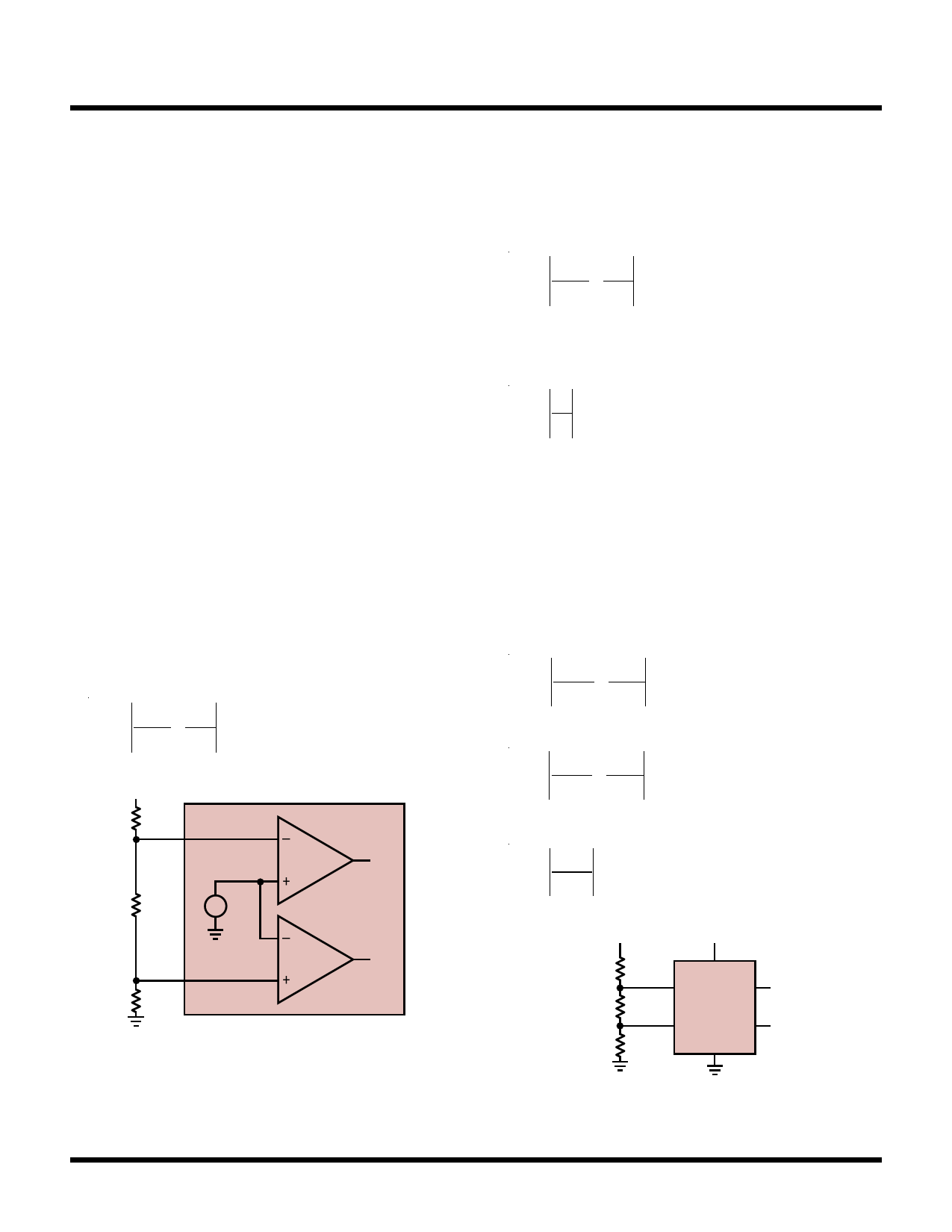
The LTC2912 is a low power voltage monitoring circuit
with an undervoltage and an overvoltage input. A timeout
period that holds OV and UV asserted after a fault has
cleared is adjustable using an external capacitor and may
be externally disabled. When configured to monitor a posi‑
tive voltage Vn using the 3‑resistor circuit configuration
shown in Figure 1, VH will be connected to the high side
tap of the resistive divider and VL will be connected to the
low side tap of the resistive divider.
3-Step Design Procedure
The following 3-step design procedure allows selecting
appropriate resistances to obtain the desired UV and OV
trip points for the voltage monitor circuit in Figure 1.
For supply monitoring, Vn is the desired nominal operat‑
ing voltage, In is the desired nominal current through the
resistive divider, VOV is the desired overvoltage trip point
and VUV is the desired undervoltage trip point.
1. Choose RA to obtain the desired OV trip point
RA is chosen to set the desired trip point for the over‑
voltage monitor.
RA
=
0.5V
In
•
Vn
VOV
(1)
Vn
RC
LTC2912
VH
–
UV
+
RB
+– 0.5V
–
VL
+
RA
OV
2912 F01
Figure 1. 3-Resistor Positive UV/OV Monitoring Configuration
2. Choose RB to obtain the desired UV trip point
Once RA is known, RB is chosen to set the desired trip
point for the undervoltage monitor.
RB =
0.5V
In
• Vn
VUV
– RA
(2)
3. Choose RC to complete the design
Once RA and RB are known, RC is determined by:
RC =
Vn
In
– RA – RB
(3)
If any of the variables Vn, In, VUV or VOV change, then each
step must be recalculated.
Voltage Monitor Example
A typical voltage monitor application is shown in Figure 2.
The monitored voltage is a 5V ±10% supply. Nominal
current in the resistive divider is 10µA.
1. Find RA to set the OV trip point of the monitor.
RA
=
0.5V
10µA
• 5V
5.5V
≈ 45.3k
2. Find RB to set the UV trip point of the monitor.
RB
=
0.5V
10µA
•
5V
4.5V
– 45.3k
≅ 10.2k
3. Determine RC to complete the design.
RC
=
5V
10µA
–
45.3k − 10.2k
≈
442k
V1
VCC
5V ±10%
5V
RC
442k
RB
10.2k
RA
45.3k
VCC
VH1
OV
LTC2912-1
VL1
UV
GND
2912 F02
Figure 2. Typical Supply Monitor
Rev. C
8
For more information www.analog.com
Share Link: 