LT1374IT7(RevA) データシートの表示(PDF) - Linear Technology
部品番号
コンポーネント説明
メーカー
LT1374IT7 Datasheet PDF : 28 Pages
| |||
LT1374
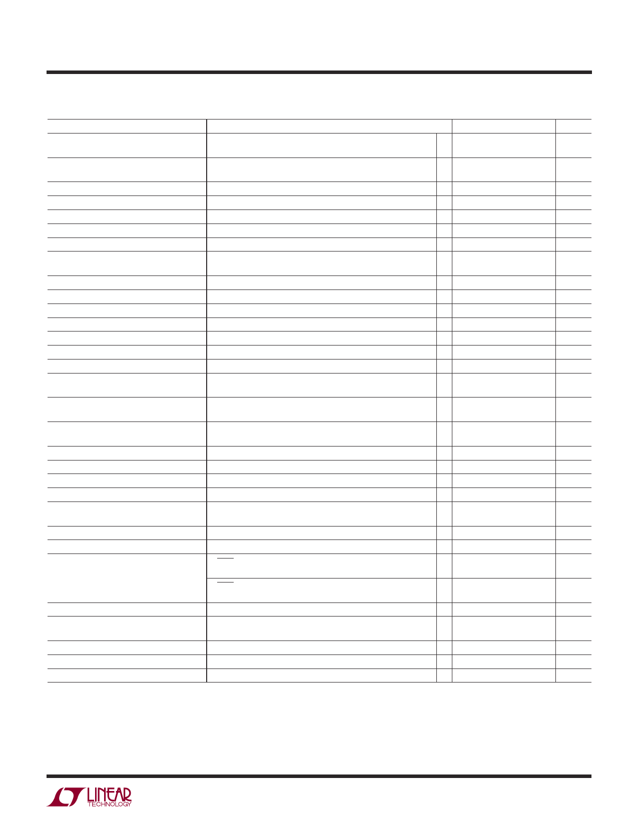
ELECTRICAL CHARACTERISTICS The q denotes specifications which apply over the full operating tempera-
ture range, otherwise specifications are at TJ = 25°C. VIN = 15V, VC = 1.5V, Boost = VIN + 5V, switch open, unless otherwise noted.
PARAMETER
Feedback Input Bias Current
Error Amplifier Voltage Gain
Error Amplifier Transconductance
CONDITIONS
(Notes 2, 8)
∆I (VC) = ±10µA (Note 8)
VC Pin to Switch Current Transconductance
Error Amplifier Source Current
Error Amplifier Sink Current
VC Pin Switching Threshold
VC Pin High Clamp
Switch Current Limit
Slope Compensation (Note 9)
Switch On Resistance (Note 7)
VFB = 2.1V or VSENSE = 4.4V
VFB = 2.7V or VSENSE = 5.6V
Duty Cycle = 0
VC Open, VFB = 2.1V or VSENSE = 4.4V, DC ≤ 50%
DC = 80%
ISW = 4.5A
Maximum Switch Duty Cycle
VFB = 2.1V or VSENSE = 4.4V
Switch Frequency
VC Set to Give 50% Duty Cycle
Switch Frequency Line Regulation
Frequency Shifting Threshold on FB Pin
Minimum Input Voltage (Note 3)
Minimum Boost Voltage (Note 4)
Boost Current (Note 5)
VIN Supply Current (Note 6)
BIAS Supply Current (Note 6)
Shutdown Supply Current
5V ≤ VIN ≤ 25V, (5V ≤ VIN ≤ 32V for LT1374HV)
∆f = 10kHz
ISW ≤ 4.5A
ISW = 1A
ISW = 4.5A
VBIAS = 5V
VBIAS = 5V
VSHDN = 0V, VIN ≤ 25V, VSW = 0V, VC Open
VSHDN = 0V, VIN ≤ 32V, VSW = 0V, VC Open
Lockout Threshold
Shutdown Thresholds
Synchronization Threshold
Synchronizing Range
SYNC Pin Input Resistance
VC Open
VC Open Device Shutting Down
Device Starting Up
MIN TYP MAX
q
0.5 2
200 400
1500 2000 2700
q 1000
3100
5.3
q 140 225 320
q 140 225 320
0.9
2.1
q 4.5 6 8.5
0.8
0.07 0.1
q
0.13
90 93
q 86 93
460 500 540
q 440
560
q
0 0.15
q 0.8 1.0 1.3
q
5.0 5.5
q
2.3 3.0
q
20 35
q
90 140
q
0.9 1.4
q
3.2 4.0
20 50
q
75
30 75
q
100
q 2.3 2.38 2.46
q 0.13 0.37 0.60
q 0.25 0.45 0.7
q
1.5 2.2
580
1000
40
UNITS
µA
µMho
µMho
A/ V
µA
µA
V
V
A
A
Ω
Ω
%
%
kHz
kHz
%/ V
V
V
V
mA
mA
mA
mA
µA
µA
µA
µA
V
V
V
V
kHz
kΩ
Note 1: Absolute Maximum Ratings are those values beyond which the life
of a device may be impaired.
Note 2: Gain is measured with a VC swing equal to 200mV above the
switching threshold level to 200mV below the upper clamp level.
Note 3: Minimum input voltage is not measured directly, but is guaranteed
by other tests. It is defined as the voltage where internal bias lines are still
regulated so that the reference voltage and oscillator frequency remain
constant. Actual minimum input voltage to maintain a regulated output will
depend on output voltage and load current. See Applications Information.
Note 4: This is the minimum voltage across the boost capacitor needed to
guarantee full saturation of the internal power switch.
Note 5: Boost current is the current flowing into the boost pin with the pin
held 5V above input voltage. It flows only during switch on time.
Note 6: VIN supply current is the current drawn when the BIAS pin is held
at 5V and switching is disabled. If the BIAS pin is unavailable or open
circuit, the sum of VIN and BIAS supply currents will be drawn by the VIN
pin.
Note 7: Switch on resistance is calculated by dividing VIN to VSW voltage
by the forced current (4.5A). See Typical Performance Characteristics for
the graph of switch voltage at other currents.
Note 8: Transconductance and voltage gain refer to the internal amplifier
exclusive of the voltage divider. To calculate gain and transconductance,
refer to the SENSE pin on the fixed voltage parts. Divide values shown by
the ratio VOUT/2.42.
Note 9: Slope compensation is the current subtracted from the switch
current limit at 80% duty cycle. See Maximum Output Load Current in the
Applications Information section for further details.
3
Share Link: 