NCE65T900 データシートの表示(PDF) - Shanghai Leiditech Electronic Technology Co., Ltd
部品番号
コンポーネント説明
メーカー
NCE65T900 Datasheet PDF : 9 Pages
| |||
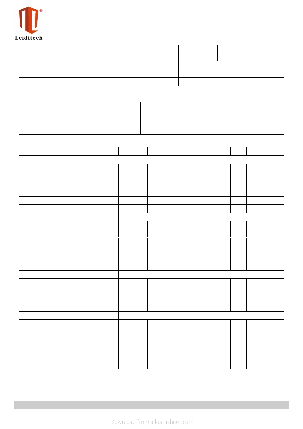
NCE65T900D,NCE65T900, NCE65T900F
Parameter
Drain Source voltage slope, VDS ≤480 V,
Reverse diode dv/dt,VDS ≤480 V,ISD<ID
Operating Junction and Storage Temperature Range
* limited by maximum junction temperature
Table 2. Thermal Characteristic
Parameter
Thermal Resistance,Junction-to-Case(Maximum)
Thermal Resistance,Junction-to-Ambient (Maximum)
Symbol
dv/dt
dv/dt
TJ,TSTG
Symbol
RthJC
RthJA
LCE65 T900
LCE65 T900F
LCE65 T900D
50
15
-55...+150
Unit
V/ns
V/ns
°C
LCE65 T900
LCE65 T900F
LCE65 T900D
2.72
4.3
62
80
Unit
°C /W
°C /W
Table 3. Electrical Characteristics (TA=25℃unless otherwise noted)
Parameter
Symbol
Condition
Min Typ
On/off states
Drain-Source Breakdown Voltage
BVDSS
VGS=0V ID=250μA
650
Zero Gate Voltage Drain Current(Tc=25℃)
IDSS
VDS=650V,VGS=0V
Zero Gate Voltage Drain Current(Tc=125℃)
IDSS
VDS=650V,VGS=0V
Gate-Body Leakage Current
IGSS
VGS=±20V,VDS=0V
Gate Threshold Voltage
VGS(th)
VDS=VGS,ID=250μA
3
Drain-Source On-State Resistance
RDS(ON)
VGS=10V, ID=2.5A
750
Dynamic Characteristics
Input Capacitance
Output Capacitance
Reverse Transfer Capacitance
Clss
370
VDS=50V,VGS=0V,
Coss
25
F=1.0MHz
Crss
0.5
Total Gate Charge
Gate-Source Charge
Gate-Drain Charge
Qg
VDS=480V,ID=5A,
Qgs
VGS=10V
Qgd
10.5
2.6
5.3
Switching times
Turn-on Delay Time
td(on)
7
Turn-on Rise Time
tr
VDD=380V,ID=3A,
3
Turn-Off Delay Time
td(off)
RG=5Ω,VGS=10V
52
Turn-Off Fall Time
tf
10
Source- Drain Diode Characteristics
Source-drain current(Body Diode)
ISD
Pulsed Source-drain current(Body Diode)
ISDM
TC=25°C
Forward on voltage
VSD
Tj=25°C,ISD=5A,VGS=0V
0.9
Reverse Recovery Time
trr
210
Reverse Recovery Charge
Qrr
Tj=25°C,IF=2.5A,di/dt=100A/μs
0.66
Peak reverse recovery current
Irrm
6.5
Notes: 1.Repetitive Rating: Pulse width limited by maximum junction temperature
2. Tj=25℃,VDD=50V,VG=10V, RG=25Ω
Max
1
50
±100
4
900
15
62
16
5
20
1.2
Unit
V
μA
μA
nA
V
mΩ
pF
pF
pF
nC
nC
nC
nS
nS
nS
nS
A
A
V
nS
uC
A
Rev :01.06.2018
2/9
www.leiditech.com
Share Link: 