ADSQ-1410 データシートの表示(PDF) - Murata Power Solutions
部品番号
コンポーネント説明
メーカー
ADSQ-1410 Datasheet PDF : 11 Pages
| |||
FUNCTIONAL SPECIFICATIONS, CONT.
Power Requirements
Power Supply Ranges
+5VEE Supply
–5VCC Supply
+VDD Supply
+4.75 +5.0 +5.25 Volts
–5.25 –5.0 –4.75 Volts
+2V +3.3 +5V
Volts
Power Supply Currents
+5V Supply
–5V Supply
+VDD Supply
–
390 430
mA
–
140 155
mA
–
12
20
mA
Power Dissipation
–
2.7
3.1
Watt
Power Supply Rejection
(5%) @25°C
–
– ±0.01 %FSR/%V
Environmental
Operating Temperature Range
ADSQ-1410
0
–
+70
°C
ADSQ-1410EX
TBD
–
TBD
°C
Storage Temperature
–65
–
+125
°C
Package Type
66-Pin, SMT, TDIP
Weight
23 grams
PCB
FR-4 RoHS TG 170°C UL94-VO
Plastic Shell
Nylon 46, 30% GFR, Stanyl, UL94-VO
Pins
0.020 Sq. Au Plate Phosphor Bronze
TECHNICAL NOTES
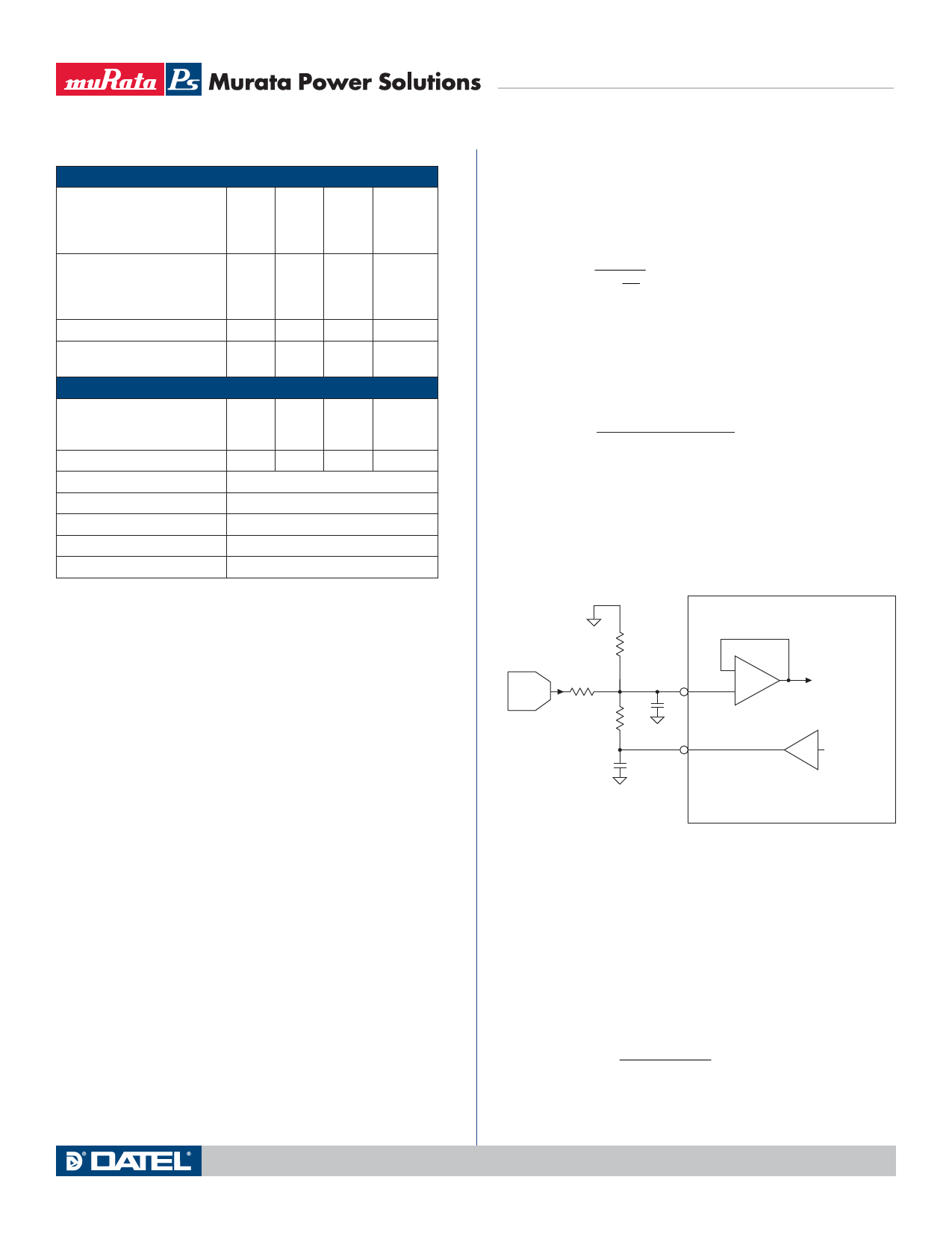
The ADSQ-1410 is a designed to function as four-independent sampling
A/D converters each with a selectable analog input range of ±1 to ±2.5
Volts and with independent offset and gain capabilities. Each channel of
the ADSQ-1410 operates from its independent +5V supplies and analog
grounds (AGND & SGND). Channels A&B share a common -5V, +VDD and
OGND_AB (output ground), similarly channels C&D share -5V, +VDD and
OGND_CD. This separation of channels along with strategically placed
ground connections within the ADSQ-1410 provide the excellent channel-
to-channel isolation performance. For optimal performance PCB layout
and high-speed / high resolution design practices should be observed.
See Layout Considerations.
RANGE & FINE GAIN ADJUSTMENT:
The ADSQ-1410 allows the full-scale range of each individual channel
to be adjusted from 2Vpp to 5Vpp. The ADSQ-1410 provides a precision
+2.5V reference voltage that can be used with a resistor divider network
to set each channel's desired full-scale range. The voltage applied to each
individual RANGE pin will set the full-scale input of that channel to be:
FS = 2 x RANGE pin voltage.
Fine Gain adjustment can be attained with precision changes to the high
impedance RANGE pins using a resistor divider network in conjunction
with a DAC or adjustable voltage source as shown in the Gain Adjust
figure.
Setting the RANGE voltage and providing the proper amount of gain
adjustment can be calculated using the following equations as referred to
the circuitry shown in the Gain Adjust figure.
ADSQ-1410
Quad 14-Bit, 10 MSPS Sampling A/D Converter
The fine gain adjustment range is equivalent to the amount of change
induced at the RANGE pin. With the desired Fine Gain Adjustment (as a
percent of full scale) and the maximum voltage expected from the Fine
Gain Adjust circuitry known, and we select a value for R1 that minimizes
the amount of current draw from Vref (typically 1kΩ range), we can then
calculate the value for R3 to be:
Eq. 1:
R3 = R1 Vtrim
Vref
%
100
Where: Vtrim = the maximum Fine Gain Adjust voltage
% = the percentage of desired trim range as a % of full scale
Defining RANGE as the unadjusted RANGE pin voltage (R3 tied to GND or
Fine Gain Adjust = 0V), we can determine the value of R2 using the follow-
ing equation:
Eq. 2: R2 =
R1 R3 Range
R3 Vref – Range (R1 + R3)
Where: RANGE is the unadjusted RANGE pin voltage
For example: Using the circuit shown, a ± 1V output DAC is used to adjust
the gain of a channel with an analog input range of ±2.0V by ± 5%.
Resistor R1 is selected to be 1k Ohm. From Eq. 1: R3 = (1k x 1.0) / (2.0
x 0.05) = 8k Ohm. For an analog input range of ±2.0V the unadjusted
RANGE voltage must be +2.0V. From Eq. 2: R2 = (1k x 8k x 2.0) / (8k x
2.5 - 2.0(1k +8k)) = 8k.
Fine Gain
Adjust
R2
R3
RANGE_A
R1
+2.5V REF
Typical for all channels
Channel A
A/D Range Select
(FS = 2 x VRANGE)
+2.5V REF
ADSQ-1410 Range / Gain Adjust
OFFSET ADJUSTMENT
Offset adjustment is accomplished by applying a ± voltage to the OFFSET
ADJ circuitry as seen in the Input Stage figure. Offset adjustment calcula-
tions can be determined using the following equations. It should be noted
that the factory trims that are required in several of the converter’s input
stages will slightly alter the tolerance of the offset adjustment calcula-
tions. For Eq. 3 the number of desired codes of adjustment are inserted
to determine the necessary voltage at the OFFSET ADJ pin. For example
with RANGE voltage = 2.5 volts and ±78 codes of adjustment desired cor-
responds to ±1V at the OFFSET ADJ pin.
Eq. 3: Voffset = 2 Range (Codes)
0.0238
Where: RANGE = the RANGE pin voltage
Codes = Desired offset adjustment range
www.murata-ps.com
Technical enquiries email: data.acquisition@murata-ps.com, tel: +1 508 339 3000
MDA_ADSQ.B01 Page 3 of 11
Share Link: 