SD103AX データシートの表示(PDF) - Shanghai Leiditech Electronic Technology Co., Ltd
部品番号
コンポーネント説明
メーカー
SD103AX Datasheet PDF : 5 Pages
| |||
SD103AX
FEATURES
Low Forward Voltage Drop
Guard Ring Construction for Transient Protection
Low Reverse Recovery Time
Low Reverse Capacitance
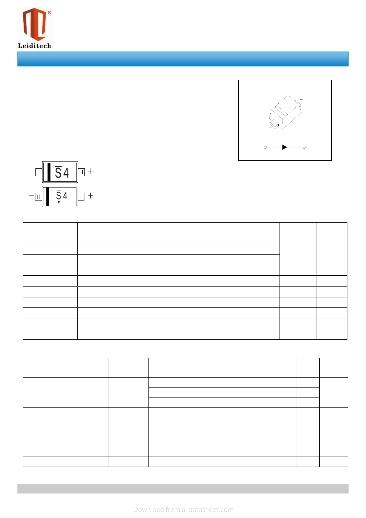
SOD-523
___
MARKING: S4
S4
S4
The marking bar indicates the cathode
Solid dot = Green molding compound device,if none, the normal device.
MAXIMUM RATINGS ( Ta=25℃ unless otherwise noted )
Symbol
Parameter
VRRM
Peak Repetitive Reverse Voltage
VRWM
Working Peak Reverse Voltage
VR
DC Blocking Voltage
VR(RMS)
RMS Reverse Voltage
IFM
Forward Continuous Current
IFSM
Non-Repetitive Peak Forward Surge Current@t=8.3ms
PD
Power Dissipation
RΘJA
Thermal Resistance From Junction To Ambient
Tj
Junction Temperature
Tstg
Storage Temperature
Value
Unit
40
V
28
200
2
150
667
125
-55~+150
V
mA
A
mW
℃/W
℃
℃
ELECTRICAL CHARACTERISTICS(Ta=25℃ unless otherwise specified)
Parameter
Reverse voltage
Reverse current
Forward voltage
Total capacitance
Reverse recovery time
Symbol
V(BR)
IR
VF
Ctot
trr
Test conditions
IR=100μA
VR=30V
VR=20V
VR=10V
IF=1mA
IF=5mA
IF=20mA
IF=200mA
VR=0V,f=1MHz
IF= IR=200mA, Irr=0.1×IR, RL=100Ω
Min Typ Max Unit
40
V
5
2
μA
1
0.27
0.32
V
0.37
0.6
50
pF
10
ns
Rev : 01.06.2015
1/5
www.leiditech.com
Share Link: 