MPC9120SD データシートの表示(PDF) - Motorola => Freescale
部品番号
コンポーネント説明
メーカー
MPC9120SD Datasheet PDF : 6 Pages
| |||

MPC9120
I2C Interface
The device has an I2C serial bus interface consisting of a
serial clock input (SCLK) and a data line (SDATA) . The clock
driver acts as a slave receiver on the I2C bus with a standard
data transfer rate of up to 100 kbit/s. The MPC9120 is a ‘write
only’ device which will not respond to general call requests
from the bus master. The I2C interface transfers data in byte
length packets except for the start, stop and acknowledge
bits. The clock driver supports block writes consisting of the
following elements.
1) Start Bit
2) Address
3) Acknowledge Bit
4) Command Code
5) Acknowledge Bit
6) Byte Count
7) Acknowledge Bit
8) Data Fields (see Table 2)
9) Acknowledge Bit
10) Stop Bit
After each byte, the clock driver pulls down the data line to
acknowledge the transfer. The clock driver holds SDATA low
during the high state of SCLK. The 7–bit address of the clock
driver is:
A7 A6 A5 A4 A3 A2 A1 R/W
11010010
Note: A7 is the first address bit
The ‘Command Code’ should be set to all ‘0’s and the
‘Byte Count’ can range from 1 to 3. The data fields are
transferred sequentially in ascending order starting with Byte
0 – Configuration Function.
The MPC9120 is compliant with the DC/AC
characteristics of a “Standard–Mode” I2C bus device. The
logic thresholds are dependent on the 3.3V supply. For
additional information on the I2C bus, refer to the document,
3114 – “The I2C–bus and how to use it (including
specifications)” available from Philips Semiconductors:
http://www.semiconductors.philips.com
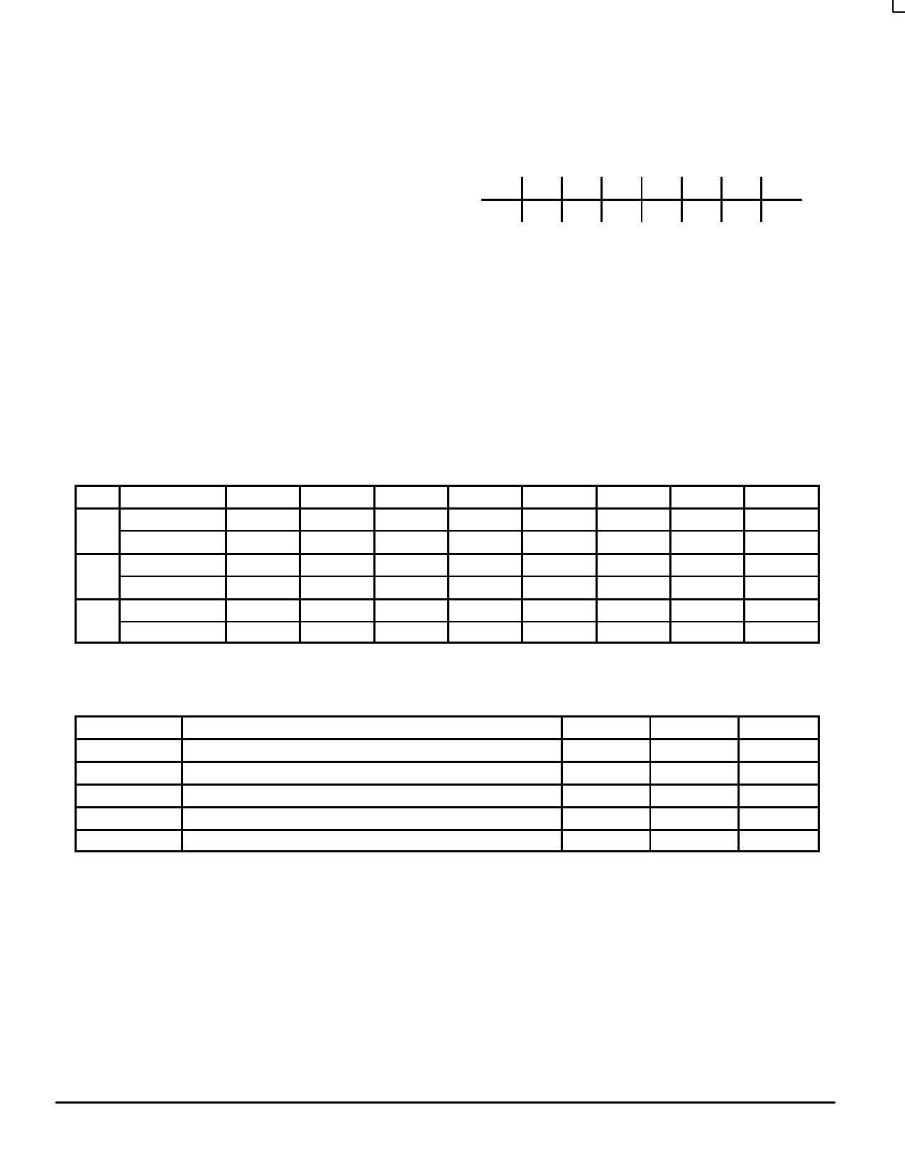
Table 2. Serial Data Fields
Byte
Function
Bit 7
Bit 6
Bit 5
Bit 4
Bit 3
Bit 2
Bit 1
SDRAM0:3
Not Used Not Used Not Used Not Used SDRAM3 SDRAM2 SDRAM1
0
Package Pin
N/A
N/A
N/A
N/A
7
6
3
SDRAM6:9
SDRAM9 SDRAM8 SDRAM7 SDRAM6 Not Used Not Used Not Used
1
Package Pin
27
26
23
22
N/A
N/A
N/A
SDRAM4:5
SDRAM5 SDRAM4 Not Used Not Used Not Used Not Used Not Used
2
Package Pin
18
11
N/A
N/A
N/A
N/A
N/A
1. Not Used bits fields are “Don’t Care” conditions.
2. When a bit field is programmed with a “1” (enable), the clock is active. A “0” (disable) means the clock is inactive.
Bit 0
SDRAM0
2
Not Used
N/A
Not Used
N/A
MAXIMUM RATINGS*
Symbol
Parameter
Min
Max
Unit
VDD
3.3V Core Supply Voltage
–0.5
4.6
V
Tstg
VIH
VIL
ESD
Storage Temperature Range
3.3V Input High Voltage (Note 3.)
3.3V Input Low Voltage
ESD Input Protection
–65
150
°C
–0.5
4.6
V
–0.5
V
2000
V
* Maximum Ratings are those values beyond which damage to the device may occur. Functional operation should be restricted to the
Recommended Operating Conditions.
3. VIH should not exceed VDD level.
TIMING SOLUTIONS
3
BR1333 — REV 5
MOTOROLA