LG1626DXC データシートの表示(PDF) - Agere -> LSI Corporation
部品番号
コンポーネント説明
メーカー
LG1626DXC Datasheet PDF : 10 Pages
| |||
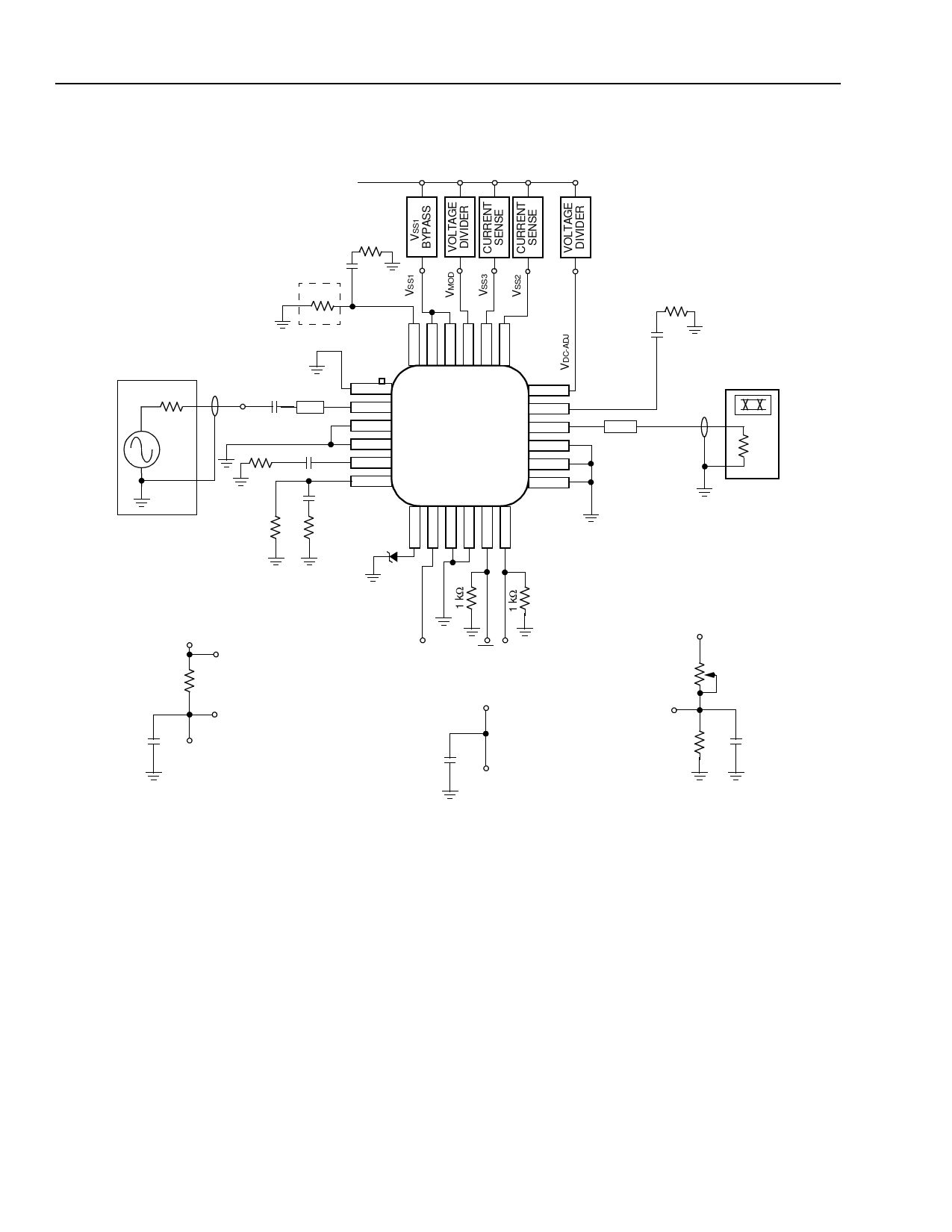
LG1626DXC Modulator Driver
Electrical Characteristics (continued)
Data Sheet
February 1999
VSS = –5.2 V
10 Ω
0.1 µF
2.5 kΩ*
VTH
+ 50 Ω
DATA IN 0.047 µF
VIN
Zo = 50 Ω
0.047 µF
50 Ω
0.1 µF
DATA
GENERATOR
2.5 kΩ
10 Ω
24 23 22 21 20 19
1
18
2
17
LG1626DXC
3
MODULATOR 16
4
DRIVER
15
5
14
6
13
7 8 9 10 11 12
BG2P5
10 Ω
0.1 µF
VOUT-DC
VOUT
Zo = 50 Ω
50 Ω
SCOPE
VSS
CURRENT
SENSE
1Ω
TO USER-SUPPLIED
VOLTAGE MONITOR
(DVM).
LM4040
MOD_5
VSS = –5.2 V
MK MK
BYPASS
FOR VSS1
VSS
VOLTAGE
DIVIDER
VSS
2 kΩ
0.1 µF
TO NODE
VSS2 AND VSS3
ONE EACH.
0.1 µF
VSS1
3 kΩ
0.1 µF
REQUIRED TO SET
VMOD AND VDC-ADJ
TO ACHIEVE DESIRED
MODULATION, ONE EACH.
5-6553(F).b
*A 2.5 kΩ resistor will set the eye crossing at 50%. A 5 kΩ potentiometer will allow the eye crossing to be varied.
Notes:
All bypass caps should be mounted close to the package.
ISS3 can be measured and used to control VMOD.
ISS2 can be measured and used to control VOUT-DC.
For optimal performance, the proximity of the two components should be minimized and the package bottom must be soldered to the circuit
board (GND).
For proper impedance matching, high-speed transmission lines should be 50 Ω controlled impedance lines.
Figure 4. LG1626DXC Typical Electrical Evaluation (ac Coupled to Scope)
6
Lucent Technologies Inc.
Share Link: 