AD9841A データシートの表示(PDF) - Analog Devices
部品番号
コンポーネント説明
メーカー
AD9841A Datasheet PDF : 23 Pages
| |||
AD9841A/AD9842A
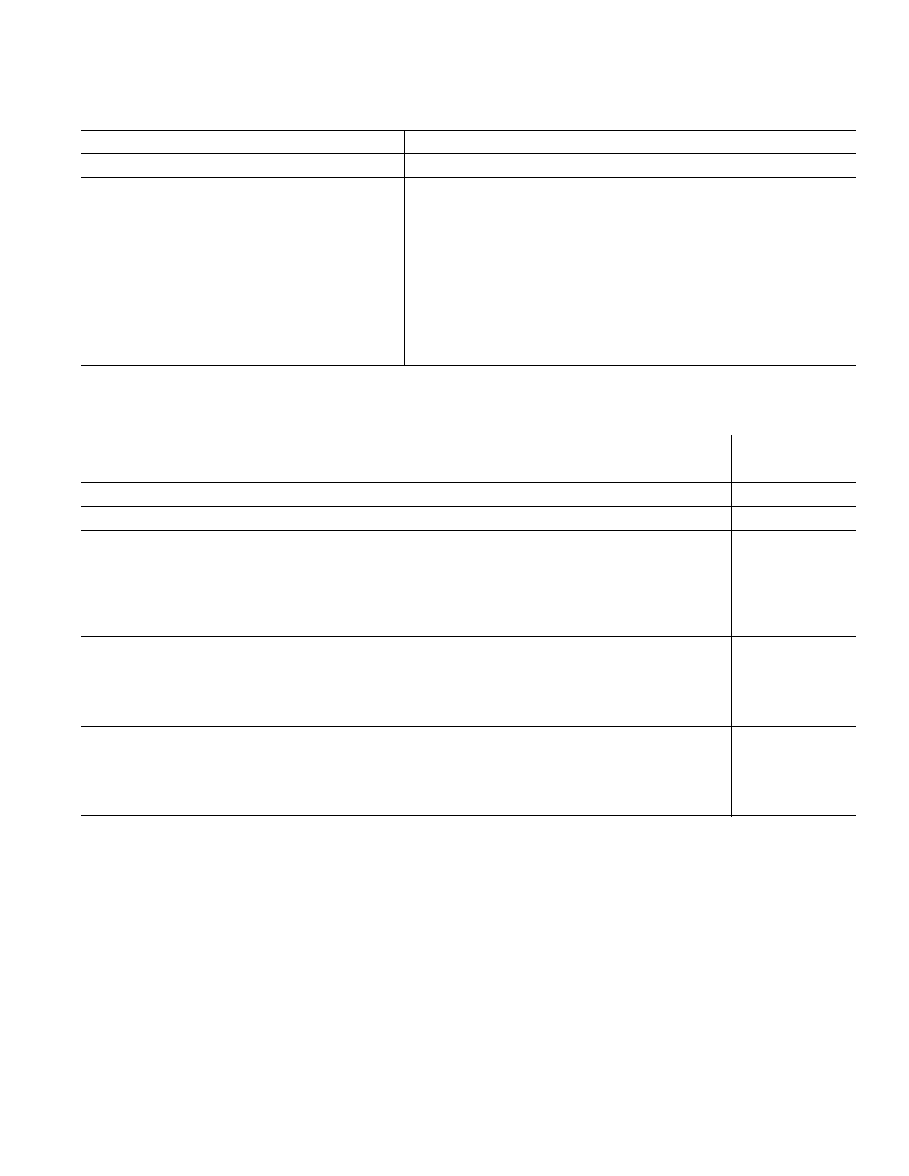
AUX1-MODE SPECIFICATIONS (TMIN to TMAX, AVDD = DVDD = 3.0 V, fDATACLK = 20 MHz, unless otherwise noted.)
Parameter
Min
POWER CONSUMPTION
MAXIMUM CLOCK RATE
20
INPUT BUFFER
Gain
Max Input Range
1.0
VGA
Max Output Range
2.0
Gain Control Resolution
Gain (Selected Using VGA Gain Register)
Min Gain
Max Gain
Specifications subject to change without notice.
Typ
Max
Unit
60
mW
MHz
0
dB
V p-p
1023
0
36
V p-p
Steps
dB
dB
AUX2-MODE SPECIFICATIONS (TMIN to TMAX, AVDD = DVDD = 3.0 V, fDATACLK = 20 MHz, unless otherwise noted.)
Parameter
Min
Typ
Max
Unit
POWER CONSUMPTION
60
mW
MAXIMUM CLOCK RATE
20
MHz
INPUT BUFFER
(Same as AUX1-MODE)
VGA
Max Output Range
2.0
Gain Control Resolution
512
Gain (Selected Using VGA Gain Register)
Min Gain
0
Max Gain
18
V p-p
Steps
dB
dB
ACTIVE CLAMP (AD9841A)
Clamp Level Resolution
Clamp Level (Measured at ADC Output)
Min Clamp Level
Max Clamp Level
256
0
63.75
Steps
LSB
LSB
ACTIVE CLAMP (AD9842A)
Clamp Level Resolution
Clamp Level (Measured at ADC Output)
Min Clamp Level
Max Clamp Level
256
Steps
0
LSB
255
LSB
Specifications subject to change without notice.
REV. 0
–5–
Share Link: 