M29W004B データシートの表示(PDF) - STMicroelectronics
部品番号
コンポーネント説明
メーカー
M29W004B Datasheet PDF : 30 Pages
| |||
M29W004T, M29W004B
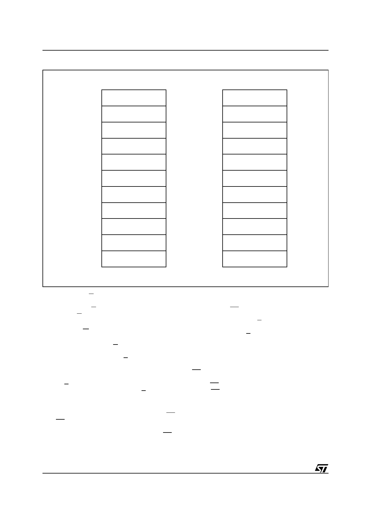
Figure 3. Memory Map and Block Address Table (x8)
7FFFFh
7C000h
7BFFFh
7A000h
79FFFh
78000h
77FFFh
70000h
6FFFFh
60000h
5FFFFh
50000h
4FFFFh
40000h
3FFFFh
30000h
2FFFFh
20000h
1FFFFh
10000h
0FFFFh
00000h
M29W004T
16K BOOT BLOCK
8K PARAMETER BLOCK
8K PARAMETER BLOCK
32K MAIN BLOCK
64K MAIN BLOCK
64K MAIN BLOCK
64K MAIN BLOCK
64K MAIN BLOCK
64K MAIN BLOCK
64K MAIN BLOCK
64K MAIN BLOCK
7FFFFh
70000h
6FFFFh
60000h
5FFFFh
50000h
4FFFFh
40000h
3FFFFh
30000h
2FFFFh
20000h
1FFFFh
10000h
0FFFFh
08000h
07FFFh
06000h
05FFFh
04000h
03FFFh
00000h
M29W004B
64K MAIN BLOCK
64K MAIN BLOCK
64K MAIN BLOCK
64K MAIN BLOCK
64K MAIN BLOCK
64K MAIN BLOCK
64K MAIN BLOCK
32K MAIN BLOCK
8K PARAMETER BLOCK
8K PARAMETER BLOCK
16K BOOT BLOCK
AI02093
Output Enable (G). The Output Enable gates the
outputs through the data buffers during a read
operation. When G is High the outputs are High
impedance. G must be forced to VID level during
Block Protection and Unprotection operations.
Write Enable (W). This input controls writing to the
Command Register and Address and Data latches.
Ready/Busy Output (RB). Ready/Busy is an
open-drain output and gives the internal state of the
P/E.C. of the device. When RB is Low, the device
is Busy with a Program or Erase operation and it
will not accept any additional program or erase
instructions except the Erase Suspend instruction.
When RB is High, the device is ready for any Read,
Program or Erase operation. The RB will also be
High when the memory is put in Erase Suspend or
Standby modes.
Reset/Block Temporary Unprotect Input (RP).
The RP Input provides hardware reset and pro-
tected block(s) temporary unprotection functions.
Reset of the memory is acheived by pulling RP to
VIL for at least tPLPX. When the reset pulse is given,
if the memory is in Read or Standby modes, it will
be available for new operations in tPHEL after the
rising edge of RP. If the memory is in Erase, Erase
Suspend or Program modes the reset will take
tPLYH during which the RB signal will be held at VIL.
The end of the memory reset will be indicated by
the rising edge of RB. A hardware reset during an
Erase or Program operation will corrupt the data
being programmed or the sector(s) being erased.
See Table 14 and Figure 9.
Temporary block unprotection is made by holding
RP at VID. In this condition previously protected
blocks can be programmed or erased. The transi-
tion of RP from VIH to VID must slower than tPHPHH.
When RP is returned from VID to VIH all blocks
temporarily unprotected will be again protected.
See Table 15 and Figure 9.
VCC Supply Voltage. The power supply for all
operations (Read, Program and Erase).
VSS Ground. VSS is the reference for all voltage
measurements.
4/30
Share Link: 