SP8855E データシートの表示(PDF) - Mitel Networks
部品番号
コンポーネント説明
メーカー
SP8855E Datasheet PDF : 14 Pages
| |||
SP8855E
Pin 19 current
VCC - 1.6V
.
Rset
Phase detector gain =
Ipin 19 (mA) X multiplication factor mA/radian
2π
To allow for control direction changes introduced by the
design of the PLL, pin 23 can be programmed to reverse the
control direction of the loop by transposing the Fpd and Fref
connections. In order that any external phase detector will also
be reversed by this function, the Fpd and Fref outputs are also
interchanged as shown in Table 2.
The charge pump connections to the loop amplifier consist
of the charge pump output and the charge pump reference.
The matching of the charge pump up and down currents will
only be maintained if the charge pumps output is held at a
voltage equal to the charge pump reference using an
operational amplifier to produce a virtual earth condition at pin
20.
The lock detect circuit can drive an LED to give visual
indication of phase lock or provide an indication to the control
system if a pull-up resistor is used in place of the LED. A small
capacitor connected from the C-lock detector pin to ground
may be used to delay lock detect indication and remove
glitches produced by momentary phase coincidence during
lock up. The phase detector can be disabled by pulling pin 39
to logic low.
Output for RF Phase Lag
Control direction pin 23
pin 20
1
Current Source
0
Current Sink
Table 2
The Fpd and Fref signals to the phase detector are available
on pin 24 and 25 and may be used to monitor the frequency
input to the phase detector or used in conjunction with an
external phase detector. When the Fpd/Fref outputs are to be
used at high frequencies, an external pull down resistor of
minimum value 330Ω may be used connected to ground to
reduce the fall time of the output pulse.
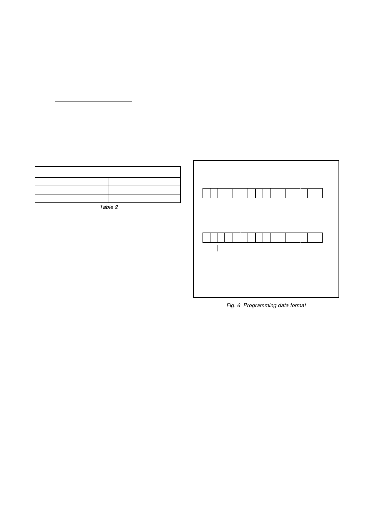
29 30 31 32 33 34 35 36 37 38 PIN
29 28 27 26 25 24 23 22 21 20
TEN BIT REFERENCE COUNTER
REFERENCE DIVIDER PROGRAMMING PIN ALLOCATION
40 41 42 43 44 1 2 3 4 5 6 7 8 9 10 11 PIN
213 212 211 210 29 28 27 26 25 24 23 22 21 20
PHASE
DETECTOR
GAIN
CONTROL
see Table 1
M COUNTER
3 BIT A
COUNTER
REFERENRCFE DIVIDER PROGRAMMING PIN ALLOCATION
Fig. 6 Programming data format
7
Share Link: 