CD4502BMS データシートの表示(PDF) - Intersil
部品番号
コンポーネント説明
メーカー
CD4502BMS Datasheet PDF : 8 Pages
| |||
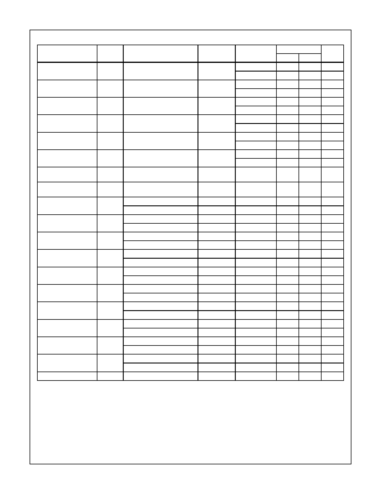
Specifications CD4502BMS
TABLE 3. ELECTRICAL PERFORMANCE CHARACTERISTICS (Continued)
LIMITS
PARAMETER
Output Current (Sink)
SYMBOL
CONDITIONS
IOL10 VDD = 10V, VOUT = 0.5V
Output Current (Sink)
IOL15 VDD = 15V, VOUT = 1.5V
Output Current (Source) IOH5A VDD = 5V, VOUT = 4.6V
Output Current (Source) IOH5B VDD = 5V, VOUT = 2.5V
Output Current (Source) IOH10 VDD = 10V, VOUT = 9.5V
Output Current (Source) IOH15 VDD =15V, VOUT = 13.5V
Input Voltage Low
Input Voltage High
Propagation Delay
Data to Output
Propagation Delay
Data to Output
Propagation Delay
Inhibit to Output
Propagation Delay
Inhibit to Output
Propagation Delay
Disable to Output
Propagation Delay
Disable to Output
Propagation Delay
Disable to Output
Propagation Delay
Disable to Output
Transition Time
Transition Time
Input Capacitance
VIL
VIH
TPHL1
TPLH1
TPHL2
TPLH2
TPHZ
TPZH
TPLZ
TPZL
TTHL
TTLH
CIN
VDD = 10V, VOH > 9V,
VOL < 1V
VDD = 10V, VOH > 9V,
VOL < 1V
VDD = 10V
VDD = 15V
VDD = 10V
VDD = 15V
VDD = 10V
VDD = 15V
VDD = 10V
VDD = 15V
VDD = 10V
VDD = 15V
VDD = 10V
VDD = 15V
VDD = 10V
VDD = 15V
VDD = 10V
VDD = 15V
VDD = 10V
VDD = 15V
VDD = 10V
VDD = 15V
Any Inputs
NOTES
1, 2, 4
1, 2, 4
1, 2
1, 2
1, 2
1, 2
1, 2
1, 2
1, 2, 3
1, 2, 3
1, 2, 3
1, 2, 3
1, 2, 3
1, 2, 3
1, 2, 3
1, 2, 3
1, 2, 4
1, 2, 4
1, 2, 4
1, 2, 4
1, 2, 4
1, 2, 4
1, 2, 4
1, 2, 4
1, 2, 3
1, 2, 3
1, 2, 3
1, 2, 3
1, 2
TEMPERATURE
+125oC
-55oC
+125oC
-55oC
+125oC
-55oC
+125oC
-55oC
+125oC
-55oC
+125oC
-55oC
+25oC, +125oC,
-55oC
+25oC, +125oC,
-55oC
+25oC
+25oC
+25oC
+25oC
+25oC
+25oC
+25oC
+25oC
+25oC
+25oC
+25oC
+25oC
+25oC
+25oC
+25oC
+25oC
+25oC
+25oC
+25oC
+25oC
+25oC
MIN
5.4
9.6
14.4
25.2
-
-
-
-
-
-
-
-
-
+7
-
-
-
-
-
-
-
-
-
-
-
-
-
-
-
-
-
-
-
-
-
MAX
-
-
-
-
-0.36
-0.64
-1.15
-2.0
-0.9
-1.6
-2.4
-4.2
3
UNITS
mA
mA
mA
mA
mA
mA
mA
mA
mA
mA
mA
mA
V
-
V
120
ns
80
ns
180
ns
130
ns
120
ns
80
ns
180
ns
130
ns
80
ns
60
ns
100
ns
80
ns
130
ns
110
ns
110
ns
80
ns
60
ns
40
ns
100
ns
80
ns
7.5
pF
NOTES:
1. All voltages referenced to device GND.
2. The parameters listed on Table 3 are controlled via design or process and are not directly tested. These parameters are characterized
on initial design release and upon design changes which would affect these characteristics.
3. CL = 50pF, RL = 200K, Input TR, TF < 20ns.
4. CL = 50pF, RL = 1K, Input TR, TF < 20ns.
7-476
Share Link: 