FS6377-01G データシートの表示(PDF) - AMI Semiconductor
部品番号
コンポーネント説明
メーカー
FS6377-01G Datasheet PDF : 21 Pages
| |||
FS6377-01/FS6377-01g Programmable 3-PLL Clock Generator IC
Data Sheet
Table 1. Pin Descriptions
Pin
Type
Name
Description
1
DIuO
SDA
Serial interface data input/output
2
DIu
SEL_CD
Selects one of two PLL C, mux D/C and post divider C/D combinations
3
DIu
PD
Power-down input
4
P
VSS
Ground
5
AI
XIN
Crystal oscillator input
6
AO
XOUT
Crystal oscillator output
7
DIu
OE
Output enable input
8
P
VDD
Power supply (5V to 3.3V)
9
DIu
ADDR
Address select
10
DO
CLK_D
D clock output
11
P
VSS
Ground
12
DO
CLK_C
C clock output
13
DO
CLK_B
B clock output
14
P
VDD
Power supply (5V to 3.3V)
15
DO
CLK_A
A clock output
16
DIu
SCL
Serial interface clock input
U
Key: AI = Analog Input; AO = Analog Output; DI = Digital Input; DI = Input With Internal Pull-Up; DID = Input With Internal Pull-Down; DIO = Digital Input/Output;
DI-3 = Three-Level Digital Input, DO = Digital Output; P = Power/Ground; # = Active Low pin
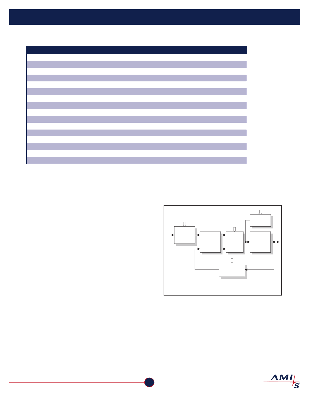
3.0 Functional Block Description
3.1 Phase Locked Loops
Each of the three on-chip phase-locked loops (PLLs) is a
standard phase- and frequency-locked loop architecture
that multiplies a reference frequency to a desired
frequency by a ratio of integers. This frequency
multiplication is exact.
As shown in Figure 3, each PLL consists of a reference
divider, a phase-frequency detector (PFD), a charge
pump, an internal loop filter, a voltage-controlled oscillator
(VCO), and a feedback divider.
During operation, the reference frequency (fREF), generated
by the on-board crystal oscillator, is first reduced by the
reference divider. The divider value is called the
"modulus," and is denoted as NR for the reference divider.
The divided reference is then fed into the PFD.
The PFD controls the frequency of the VCO (fVCO) through
the charge pump and loop filter. The VCO provides a high-
speed, low noise, continuously variable frequency clock
source for the PLL. The output of the VCO is fed back to
the PFD through the feedback divider (the modulus is
denoted by NF) to close the loop.
REFDIV[7:0]
fREF Reference
Divider
(NR)
CP
Phase-
Frequency
Detector
UP
Charge
Pump
DOWN
FBKDIV[10:0]
fPD
Feedback
Divider (NF)
LFTC
Loop
Filter
Voltage fVCO
Controlled
Oscillator
Figure 3: PLL Diagram
The PFD will drive the VCO up or down in frequency until
the divided reference frequency and the divided VCO
frquency appearing at the inputs of the PFD are equal.
The input/output relationship between the reference
frequency and the VCO frequency is:
( ) fVCO = fREF
NF
NR .
AMI Semiconductor
www.amis.com
2
Share Link: 