IS41C16256 データシートの表示(PDF) - Integrated Circuit Solution Inc
部品番号
コンポーネント説明
メーカー
IS41C16256 Datasheet PDF : 20 Pages
| |||
IS41C16256
IS41LV16256
256K x 16 (4-MBIT) DYNAMIC RAM
WITH EDO PAGE MODE
FEATURES
• Extended Data-Out (EDO) Page Mode access cycle
• TTL compatible inputs and outputs; tristate I/O
• Refresh Interval: 512 cycles /8 ms
• Refresh Mode: RAS-Only, CAS-before-RAS (CBR),
Hidden
• Single power supply:
5V ± 10% (IS41C16256)
3.3V ± 10% (IS41LV16256)
• Byte Write and Byte Read operation via two CAS
• Industrial Temperature Range -40oC to 85oC
DESCRIPTION
The ICSI IS41C16256 and IS41LV16256 is a 262,144 x 16-
bit high-performance CMOS Dynamic Random Access Memo-
ries. The IS41C16256 offer an accelerated cycle access
called EDO Page Mode. EDO Page Mode allows 512 random
accesses within a single row with access cycle time as short
as 10 ns per 16-bit word. The Byte Write control, of upper and
lower byte, makes the IS41C16256 ideal for use in
16-, 32-bit wide data bus systems.
These features make the IS41C16256and IS41LV16256 ideally
suited for high-bandwidth graphics, digital signal processing,
high-performance computing systems, and peripheral
applications.
KEY TIMING PARAMETERS
Parameter
Max. RAS Access Time (tRAC)
Max. CAS Access Time (tCAC)
Max. Column Address Access Time (tAA)
Min. EDO Page Mode Cycle Time (tPC)
Min. Read/Write Cycle Time (tRC)
The IS41C16256 is packaged in a 40-pin 400mil SOJ and
400mil TSOP-2.
-25(5V)
-35
-50
-60
Unit
25
35
50
60
ns
10
10
14
15
ns
12
18
25
30
ns
10
12
20
25
ns
45
60
90
110
ns
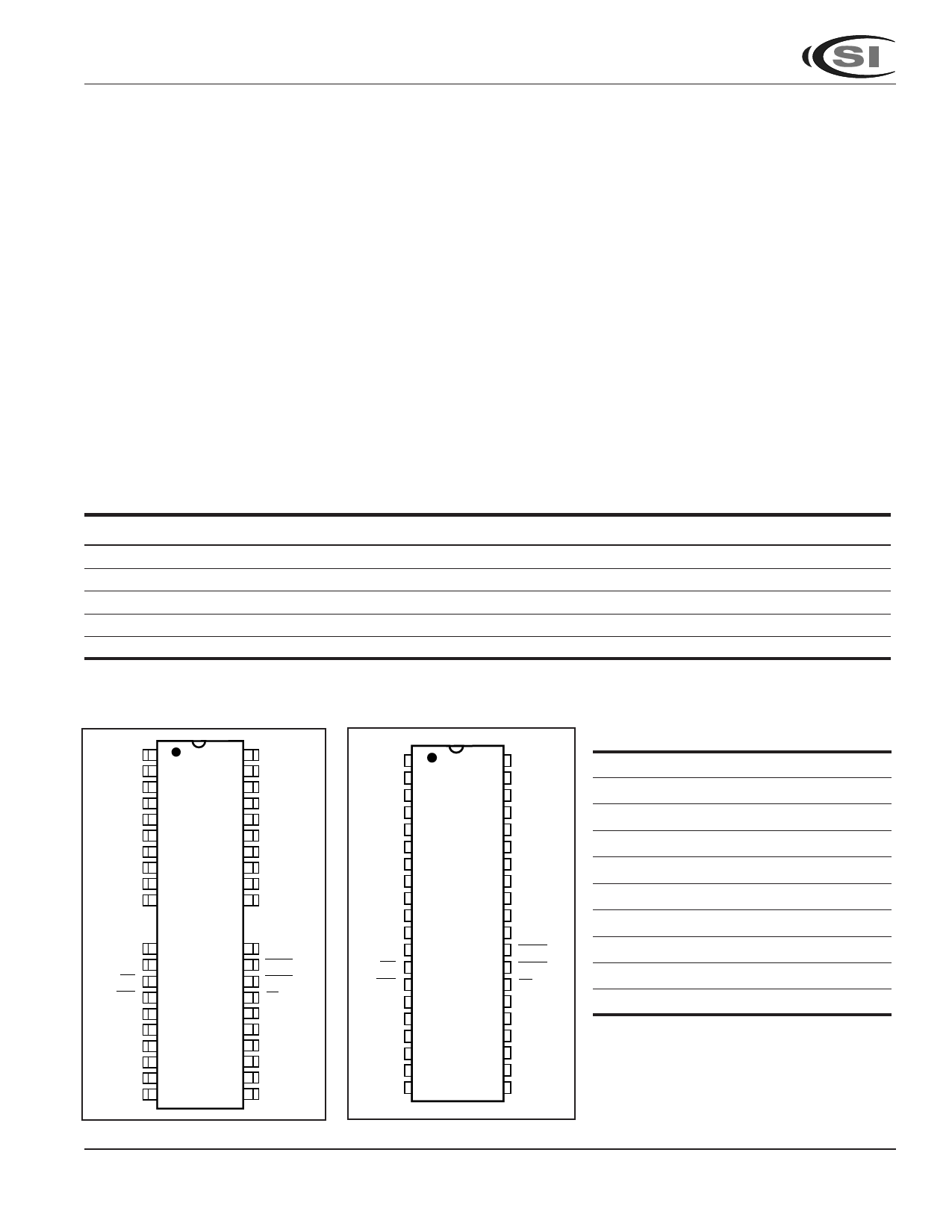
PIN CONFIGURATIONS
40-Pin TSOP-2
VCC 1
I/O0 2
I/O1 3
I/O2 4
I/O3 5
VCC 6
I/O4 7
I/O5 8
I/O6 9
I/O7 10
40 GND
39 I/O15
38 I/O14
37 I/O13
36 I/O12
35 GND
34 I/O11
33 I/O10
32 I/O9
31 I/O8
NC 11
NC 12
WE 13
RAS 14
NC 15
A0 16
A1 17
A2 18
A3 19
VCC 20
30 NC
29 LCAS
28 UCAS
27 OE
26 A8
25 A7
24 A6
23 A5
22 A4
21 GND
40-Pin SOJ
VCC 1
I/O0 2
I/O1 3
I/O2 4
I/O3 5
VCC 6
I/O4 7
I/O5 8
I/O6 9
I/O7 10
NC 11
NC 12
WE 13
RAS 14
NC 15
A0 16
A1 17
A2 18
A3 19
VCC 20
40 GND
39 I/O15
38 I/O14
37 I/O13
36 I/O12
35 GND
34 I/O11
33 I/O10
32 I/O9
31 I/O8
30 NC
29 LCAS
28 UCAS
27 OE
26 A8
25 A7
24 A6
23 A5
22 A4
21 GND
PIN DESCRIPTIONS
A0-A8
I/O0-15
WE
OE
RAS
UCAS
LCAS
Vcc
GND
NC
Address Inputs
Data Inputs/Outputs
Write Enable
Output Enable
Row Address Strobe
Upper Column Address Strobe
Lower Column Address Strobe
Power
Ground
No Connection
ICSI reserves the right to make changes to its products at any time without notice in order to improve design and supply the best possible product. We assume no responsibility for any errors
which may appear in this publication. © Copyright 2000, Integrated Circuit Solution Inc.
Integrated Circuit Solution Inc.
1
DR001-0E 01/25/2002
Share Link: 