MAX3095CSE гғҮгғјгӮҝгӮ·гғјгғҲгҒ®иЎЁзӨәпјҲPDFпјү - Maxim Integrated
йғЁе“Ғз•ӘеҸ·
гӮігғігғқгғјгғҚгғігғҲиӘ¬жҳҺ
гғЎгғјгӮ«гғј
MAX3095CSE Datasheet PDF : 11 Pages
| |||
Вұ15kV ESD-Protected, 10Mbps, 3V/5V,
Quad RS-422/RS-485 Receivers
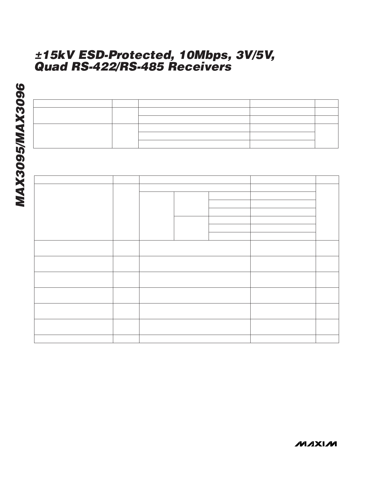
DC ELECTRICAL CHARACTERISTICSвҖ”MAX3096 (continued)
(VCC = 3.135V to 3.6V, TA = TMIN to TMAX, unless otherwise noted. Typical values are at VCC = 3.3V, TA = +25В°C.) (Note 1)
PARAMETER
SYMBOL
CONDITIONS
MIN TYP MAX UNITS
Supply Current
ESD Protection
(Note 2)
ICC
No load, G = VCC or G = GND
G = GND and G = VCC
Human Body Model
IEC1000-4-2 (Air-Gap Discharge)
IEC1000-4-2 (Contact Discharge)
2.4
4.0
mA
0.001 10
ВөA
Вұ15
Вұ15
kV
Вұ8
SWITCHING CHARACTERISTICSвҖ”MAX3096
(VCC = 3.135V to 3.6V, TA = TMIN to TMAX, unless otherwise noted. Typical values are at TA = +25В°C.)
PARAMETER
SYMBOL
CONDITIONS
MIN TYP MAX UNITS
VCC = 3.135V to 3.6V, TA = TMIN to TMAX
TA = +85В°C
69
127
88
98
112
Input-to-Output Propagation
Delay
tPLH, tPHL |VID| = 3V,
Figure 2
VCC = 3.60V
VCC = 3.135V
TA = +25В°C
TA = -40В°C
TA = +85В°C
TA = +25В°C
TA = -40В°C
78
88
102
69
79
93
ns
103
113
127
91
101
115
82
92
106
Device-to-Device Propagation-
Delay Matching
|VID| = 3V, Figure 2, matched conditions
24
ns
Propagation-Delay Skew
(tPLH - tPHL)
tSK
-2
Вұ10
ns
Output Enable Time to
Low Level
tZL
Figure 3
600 1000
ns
Output Enable Time to
High Level
tZH
Figure 3
600 1000
ns
Output Disable Time from
Low Level
tLZ
Figure 3
80
180
ns
Output Disable Time from
High Level
tHZ
Figure 3
80
180
ns
Maximum Data Rate
fMAX
10
Mbps
Note 1: All currents into the device are positive; all currents out of the device are negative. All voltages are referred to device
ground, unless otherwise noted.
Note 2: Receiver inputs (A_, B_).
4 _______________________________________________________________________________________
Share Link: 