CY7C1486V33(2004) データシートの表示(PDF) - Cypress Semiconductor
部品番号
コンポーネント説明
メーカー
CY7C1486V33 Datasheet PDF : 30 Pages
| |||
PRELIMINARY
CY7C1480V33
CY7C1482V33
CY7C1486V33
The ADV input is ignored during this cycle. If a global Write is
conducted, the data presented to the DQs is written into the
corresponding address location in the memory core. If a Byte
Write is conducted, only the selected bytes are written. Bytes
not selected during a Byte Write operation will remain
unaltered. A synchronous self-timed Write mechanism has
been provided to simplify the Write operations.
Because CY7C1480V33/CY7C1482V33/CY7C1486V33 is a
common I/O device, the Output Enable (OE) must be
deasserted HIGH before presenting data to the DQs inputs.
Doing so will tri-state the output drivers. As a safety
precaution, DQs are automatically tri-stated whenever a Write
cycle is detected, regardless of the state of OE.
Burst Sequences
The CY7C1480V33/CY7C1482V33/CY7C1486V33 provides
a two-bit wraparound counter, fed by A1: A0, that implements
either an interleaved or linear burst sequence. The interleaved
burst sequence is designed specifically to support Intel
Pentium applications. The linear burst sequence is designed
to support processors that follow a linear burst sequence. The
burst sequence is user selectable through the MODE input.
Asserting ADV LOW at clock rise will automatically increment
the burst counter to the next address in the burst sequence.
Both Read and Write burst operations are supported.
Sleep Mode
The ZZ input pin is an asynchronous input. Asserting ZZ
places the SRAM in a power conservation “sleep” mode. Two
clock cycles are required to enter into or exit from this “sleep”
mode. While in this mode, data integrity is guaranteed.
Accesses pending when entering the “sleep” mode are not
considered valid nor is the completion of the operation
guaranteed. The device must be deselected prior to entering
the “sleep” mode. CE1, CE2, CE3, ADSP, and ADSC must
remain inactive for the duration of tZZREC after the ZZ input
returns LOW.
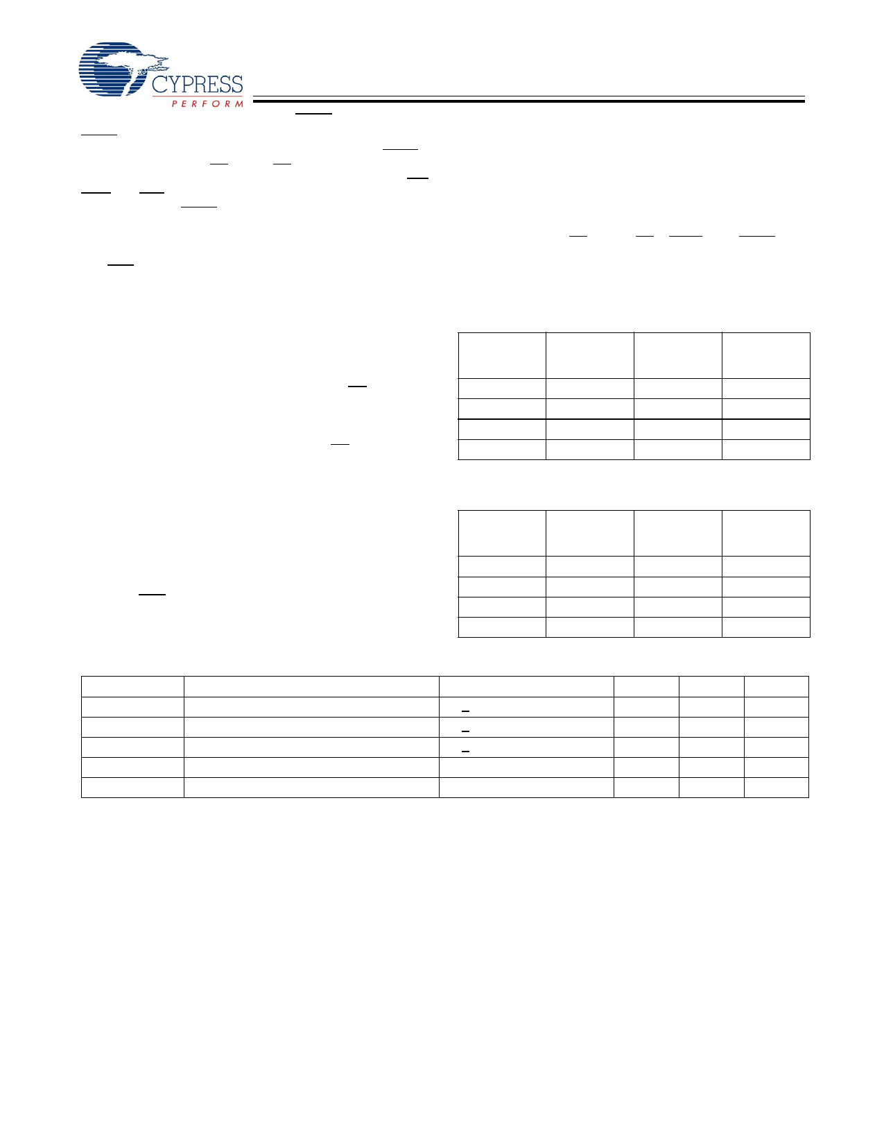
Interleaved Burst Address Table
(MODE = Floating or VDD)
First
Address
A1: A0
Second
Address
A1: A0
Third
Address
A1: A0
00
01
10
01
00
11
10
11
00
11
10
01
Fourth
Address
A1: A0
11
10
01
00
Linear Burst Address Table
(MODE = GND)
First
Address
A1: A0
00
01
10
11
Second
Address
A1: A0
01
10
11
00
Third
Address
A1: A0
10
11
00
01
Fourth
Address
A1: A0
11
00
01
10
ZZ Mode Electrical Characteristics
Parameter
IDDZZ
tZZS
tZZREC
tZZI
tRZZI
Description
Sleep mode standby current
Device operation to ZZ
ZZ recovery time
ZZ Active to Sleep current
ZZ Inactive to exit Sleep current
Test Conditions
ZZ > VDD – 0.2V
ZZ > VDD – 0.2V
ZZ < 0.2V
This parameter is sampled
This parameter is sampled
Min.
2tCYC
0
Max.
120
2tCYC
2tCYC
Unit
mA
ns
ns
ns
ns
Document #: 38-05283 Rev. *C
Page 9 of 30
Share Link: 