MT46V16M8TG-8 データシートの表示(PDF) - Micron Technology
部品番号
コンポーネント説明
メーカー
MT46V16M8TG-8 Datasheet PDF : 68 Pages
| |||
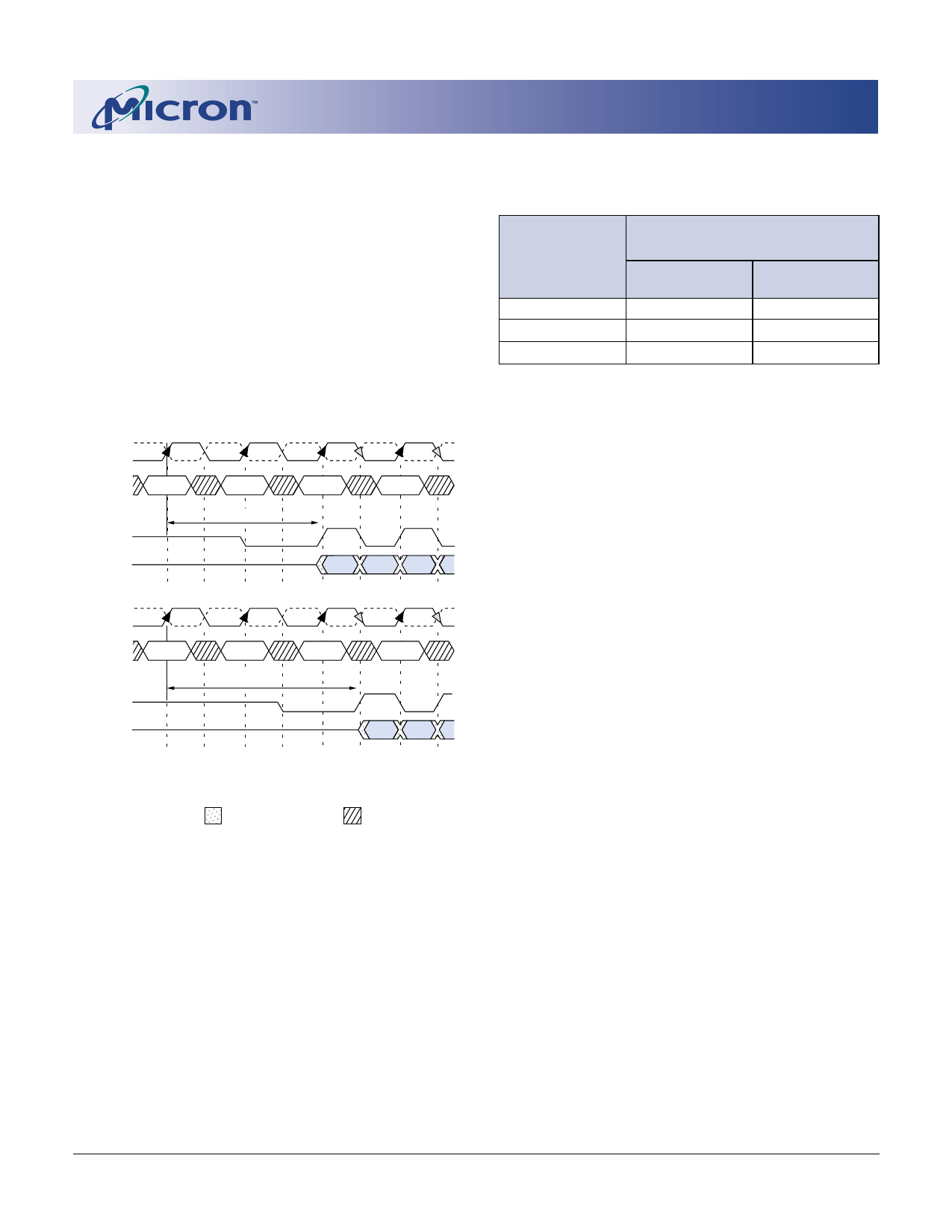
Read Latency
The READ latency is the delay, in clock cycles,
between the registration of a READ command and the
availability of the first bit of output data. The latency
can be set to 2 or 2.5 clocks, as shown in Figure 2.
If a READ command is registered at clock edge n,
and the latency is m clocks, the data will be available
nominally coincident with clock edge n + m. Table 2
indicates the operating frequencies at which each CAS
latency setting can be used.
Reserved states should not be used as unknown
operation or incompatibility with future versions may
result.
PRELIMINARY
128Mb: x4, x8, x16
DDR SDRAM
TABLE 2
CAS LATENCY (CL)
ALLOWABLE OPERATING
FREQUENCY (MHz)
SPEED
-75Z
-75
-8
CL = 2
75 ≤ f ≤ 133
75 ≤ f ≤ 100
75 ≤ f ≤ 100
CL = 2.5
75 ≤ f ≤133
75 ≤ f ≤133
75 ≤ f ≤125
CK#
CK
COMMAND
DQS
DQ
CK#
CK
COMMAND
DQS
DQ
T0
T1
READ
NOP
CL = 2
T2 T2n T3 T3n
NOP
NOP
T0
READ
T1
T2 T2n T3 T3n
NOP
NOP
NOP
CL = 2.5
Burst Length = 4 in the cases shown
Shown with nominal tAC and nominal tDSDQ
TRANSITIONING DATA
DON’T CARE
Operating Mode
The normal operating mode is selected by issuing a
MODE REGISTER SET command with bits A7-A11
each set to zero, and bits A0-A6 set to the desired values.
A DLL reset is initiated by issuing a MODE REGISTER
SET command with bits A7 and A9-A11 each set to
zero, bit A8 set to one, and bits A0-A6 set to the desired
values. Although not required by the Micron device,
JEDEC specifications recommend when a LOAD MODE
REGISTER command is issued to reset the DLL, it
should always be followed by a LOAD MODE REGIS-
TER command to select normal operating mode.
All other combinations of values for A7-A11 are
reserved for future use and/or test modes. Test modes
and reserved states should not be used because un-
known operation or incompatibility with future ver-
sions may result.
Figure 2
CAS Latency
128Mb: x4, x8, x16 DDR SDRAM
128Mx4x8x16DDR_C.p65 – Rev. C; Pub. 4/01
11
Micron Technology, Inc., reserves the right to change products or specifications without notice.
©2001, Micron Technology, Inc.
Share Link: 