AD9929 データシートの表示(PDF) - Analog Devices
部品番号
コンポーネント説明
メーカー
AD9929 Datasheet PDF : 64 Pages
| |||
AD9929
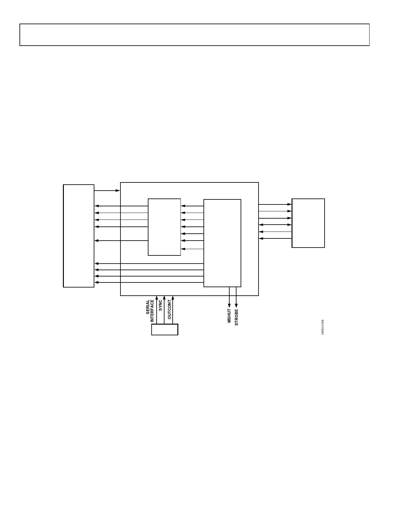
SYSTEM OVERVIEW
Figure 7 shows the typical system block diagram for the
AD9929. The CCD output is processed by the AD9929’s AFE
circuitry, which consists of a CDS, VGA, black level clamp, and
an A/D converter. The digitized pixel information is sent to the
digital image processor chip, which performs post-processing
and compression. To operate the CCD, all CCD timing para-
meters are programmed into the AD9929 from the system
microprocessor through the 3-wire serial interface. From the
system master clock, CLI, provided by the image processor or
external crystal, the AD9929 generates all of the CCDs hori-
zontal and vertical clocks and all internal AFE clocks. External
synchronization is provided by a SYNC pulse from the
microprocessor, which resets internal counters and resyn-
chronizes the VD and HD outputs.
The H-drivers for H1 to H2, and RG are included in the
AD9929, allowing these clocks to be directly connected to the
CCD. An H-drive voltage of up to 3.6 V is supported. The
AD9929 also includes the CCD vertical driver circuits for
creating the V1 to V4, and SUBCK outputs that allow direct
connection to the CCD. The AD9929 also provides program-
mable MSHUT and STROBE outputs, which may be used to
trigger mechanical shutter and strobe (flash) circuitry.
CCD
CCDIN
V1
V2
V3
V4
SUBCK
H1
H2
RG
VSUB
AD9929
VERTICAL
DRIVER
XV1
XV2
XV3
XV4
XVSG1
XVSG2
XSUBCK
TIMING
GENERATOR
DOUT [11:0]
DCLK1
FD
HD, VD
VGATE
CLI
DIGITAL
IMAGE
PROCESSING
ASIC
µP
Figure 7. Typical System Block Diagram, Master Mode
Rev. A | Page 18 of 64
Share Link: 