AN8049 データシートの表示(PDF) - Panasonic Corporation
部品番号
コンポーネント説明
メーカー
AN8049
Panasonic Corporation

AN8049 Datasheet PDF : 27 Pages
| |||
Voltage Regulators
AN8049SH
I Usage Notes
[1] Allowable power dissipation
1. Since the power dissipation (P) in this IC increases proportionally with the supply voltage, applications must be careful
to operate so that the loss does not exceed the allowable power dissipation, PD, for the package. See the PD Ta curve.
Reference formula:
P = (VCC −VBEQ1) × ISO(OUT)1 × Du1 + (VCC − VBEQ2) × ISO(OUT)2 × Du2 + VO(SAT)3 × IOUT3 × Du3 + VCC × ICC
< PD
VBEQ1 : The voltage between the base and emitter of the channel 1 npn transistor
ISO(OUT)1 : The OUT1 pin output source current
(This is set by the resistor connected to the RB1 pin. When RB is 1 kΩ, ISO(OUT)1 will be 34 mA,
maximum.)
Du1 : The output 1 on-duty
VBEQ2 : The voltage between the base and emitter of the channel 2 npn transistor
ISO(OUT)2 : The OUT2 pin output source current
(This is set by the resistor connected to the RB2 pin. When RB is 1 kΩ, ISO(OUT)2 will be 34 mA,
maximum.)
Du2 : The output 2 on-duty
VO(SAT)3 : The OUT3 pin saturation voltage (0.5 V maximum when IOUT3 is 40 mA.)
IOUT3 : The OUT3 pin current (This will be {VCC − VBEQ3 − VO(SAT)3}/RO3 .)
Du3 : The output 3 on-duty
ICC
: The VCC pin current
2. If the IC is shorted to ground, shorted to VCC, or inserted incorrectly, either the device itself or peripheral
components will be destroyed.
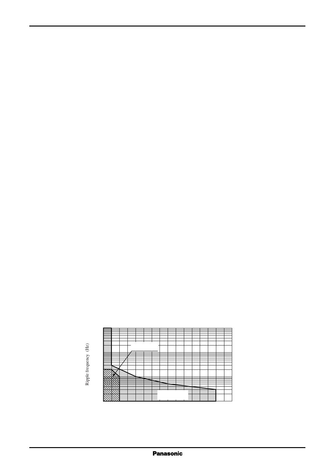
[2] Allowable VCC ripple
VCC ripple due to the switching transistor being turned on and off can cause this IC's U.V.L.O. circuit, which is
biased by VCC, to operate incorrectly, and can cause the S.C.P. capacitor charging operation to fail to start when the
output is shorted.
The figure shows the allowable range for VCC ripple. Applications should reduce VCC ripple either by inserting a
ripple filter in the VCC line or by inserting a capacitor between the IC GND and VCC pins and locating that capacitor
as close to the IC as possible.
Note that the allowable range shown here is the result of testing the IC independently, and that the allowable range
may differ depending on the actual system of the power supply circuit. Also note that this allowable range is a design
target, and is not guaranteed by testing of all samples.
Allowable VCC ripple
10M
Allowable range
when VCC is 3 V.
1M
100k
Allowable range
when VCC is 10 V.
10k
0
1
2
3
4
5
6
7
8
VCC ripple voltage VCC(AC) (V[p-p])
11
Share Link: