ATA6628 データシートの表示(PDF) - Atmel Corporation
部品番号
コンポーネント説明
メーカー
ATA6628 Datasheet PDF : 36 Pages
| |||
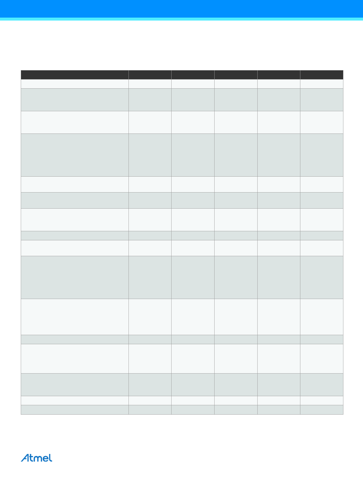
7. Absolute Maximum Ratings
Stresses beyond those listed under “Absolute Maximum Ratings” may cause permanent damage to the device. This is a stress rating
only and functional operation of the device at these or any other conditions beyond those indicated in the operational sections of this
specification is not implied. Exposure to absolute maximum rating conditions for extended periods may affect device reliability.
Parameters
Supply voltage VS
Pulse time ≤ 500ms
Ta = 25°C
Output current IVCC ≤ 85mA
Pulse time ≤ 2min
Ta = 25°C
Output current IVCC ≤ 85mA
WAKE (with 2.7kΩ serial resistor)
KL_15 (with 47kΩ/100nF)
VBATT (with 47Ω/10nF)
DC voltage
Transient voltage due to ISO7637 (coupling
1nF)
INH
- DC voltage
LIN, VBATT
- DC voltage
Logic pins (RxD, TxD, EN, NRES, NTRIG,
WD_OSC, MODE, TM, DIV_ON,
SP_MODE, PV)
Output current NRES
PVCC DC voltage
VCC DC voltage
ESD according to IBEE LIN EMC
Test Spec. 1.0 following IEC 61000-4-2
- Pin VS, LIN to GND
- Pin WAKE (2.7kΩ, serial resistor) to GND
- Pin KL_15 (47kΩ/100nF) to GND
- Pin VBATT (10nF) to GND
HBM ESD
ANSI/ESD-STM5.1
JESD22-A114
AEC-Q100 (002)
MIL-STD-883 (M3015.7)
CDM ESD STM 5.3.1
MM ESD
EIA/JESD22-A115
ESD STM5.2
AEC-Q100 (002)
ESD HBM following STM5.1 with 1.5kΩ
100pF
- Pin VS, LIN, KL_15, WAKE to GND
Junction temperature
Storage temperature
Symbol
VS
VS
VS
INRES
Tj
Ts
Min.
–0.3
–1
–150
–0.3
–27
–0.3
–0.3
–0.3
±8
±3
±750
±200
±6
–40
–55
Typ.
Max.
Unit
+40
V
+40
V
27
V
+40
V
+100
V
VS + 0.3
V
+40
V
VCC + 0.5V
V
+2
mA
+5.5
V
+6.5
V
KV
KV
V
V
KV
+150
°C
+150
°C
ATA6628/ATA6630 [DATASHEET]
21
9117I–AUTO–10/14
Share Link: 