MAX121C データシートの表示(PDF) - Maxim Integrated
部品番号
コンポーネント説明
メーカー
MAX121C Datasheet PDF : 26 Pages
| |||
MAX121
308ksps ADC with DSP Interface and 78dB SINAD
Timing and Control
The MAX121 has three possible modes of operation, as
outlined in the timing diagrams of Figures 7–9 and dis-
cussed in the Operating Modes section.
In Mode 1, the CONVST input is used to control the start
of the conversion. Mode 1 is intended for DSP and other
applications where the analog input must be sampled at
a precise instant in time.
In Mode 2, the CS input controls the start of the conver-
sion. This mode is useful when several devices are mul-
tiplexed on the same serial data bus, since the MAX121
outputs are placed in a high-impedance state when CS is
pulled high.
Mode 3 is the continuous-conversion mode. This mode
is intended for data logging and similiar applications
where the MAX121 is directly linked to memory through
a first-in/first-out (FIFO) buffer or a direct memory access
(OMA) port.
In all three operating modes, the start of conversion is
controlled by either the CS or the CONVST input. Both of
these inputs must be low for a conversion to take place.
Figure 6 shows the logic equivalent for the conversion
circuitry. Once the conversion is in progress, it cannot be
restarted.
Operating Modes
Mode 1: CONVST Controls Conversion Starts
(MODE = VDD, CS = DGND)
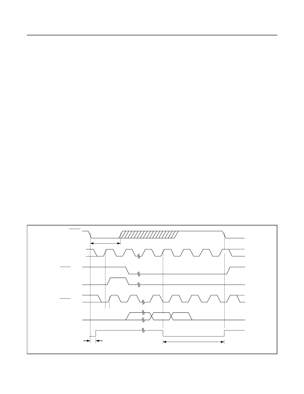
Figure 7 shows the timing diagram for mode 1. In this
mode, conversion start operations are controlled by the
CONVST input.
A falling edge on the CONVST input places the T/H into
the hold mode and starts a conversion in the successive
approximation register (SAR). The FSTRT (normally
low) output goes high on the next rising clock edge and
remains high for one clock cycle. On the next rising clock
edge, FSTRT goes low and the SFRM output goes low
(INVFRM = VDD), indicating that the MSB is ready to be
latched. SFRM remains high for 16 clock cycles ( 4 data
bits plus 2 trailing zeros).
The T/H amplifier returns to the track mode when the 14th
bit (D0) is clocked out of the SDATA pin. A new conver-
sion can be initiated by the CONVST input after the 400ns
minimum acquisition time has been satisfied.
CS must be low to start a conversion. In applications
where the MAX121 interfaces with a dedicated serial port,
CS can be hardwired to DGND. To interface the MAX121
to a multiplexed serial bus, CS can be externally driven
low to enable conversions, or driven high to place the
serial outputs into a high-impedance state.
CONVST
CLKIN
tCW
1
13
14
15
16*
17*
SFRM
(INVFRM = VDD)
FSTRT
SCLK
(INVCRM = VDD)
SDATA
1
tCD
13
14
15
16*
17*
MSB D2
D1
LSB
HOLD
T/H
TRACK
tAP
tAQ
* THESE CLOCK CYCLES MAY BE OMITTED IF THE SFRM SIGNAL IS NOT NEEDED
Figure 7. CONVST Controls Conversion Starts (Mode 1)
www.maximintegrated.com
Maxim Integrated │ 8
Share Link: 