CS61582 データシートの表示(PDF) - Cirrus Logic
部品番号
コンポーネント説明
メーカー
CS61582 Datasheet PDF : 32 Pages
| |||

shift operation. Note that if J-TDI is floating,
an internal pull-up resistor forces the pin high.
JTAG Data Registers (DR)
The test data registers are the Boundary-Scan
Register (BSR), the Device Identification Regis-
ter (DIR), and the Bypass Register (BR).
BSR bits
0-2
3-5
6
7
8-9
10-11
12-13
14-16
17-19
20
21-23
24-26
27-29
30-32
33-35
36-38
39-41
42-44
45
46-48
49-50
51-52
53-54
55
56
57-59
60-62
63
64
Pin Name
LOS1
TNEG1
TPOS1
TCLK1
RNEG1
RPOS1
RCLK1
DPM1
RLOOP1
LLOOP2
LLOOP1
TAOS1
TAOS2
CON01
CON02
CON11
CON12
CON21
CON22
DPM2
RCLK2
RPOS2
RNEG2
TCLK2
TPOS2
TNEG2
LOS2
CLKE
RLOOP2
1. Configure pad as an input.
2. Configure pad as an output.
Pad Type
bi-directional2
bi-directional1
input
input
output
output
output
bi-directional2
bi-directional1
input
bi-directional1
bi-directional1
bi-directional1
bi-directional1
bi-directional1
bi-directional1
bi-directional1
bi-directional1
input
bi-directional2
output
output
output
input
input
bi-directional1
bi-directional2
input
input
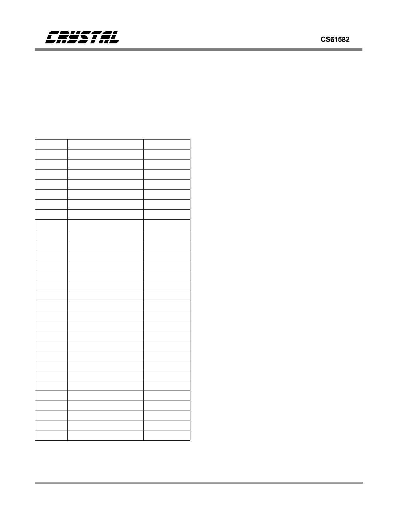
Table 3. Boundary Scan Register
14
Boundary Scan Register: The BSR is connected
in parallel to all the digital I/O pins, and pro-
vides the mechanism for applying/reading test
patterns to/from the board traces. The BSR is 65
bits long and is initialized and read using the in-
struction SAMPLE/PRELOAD. The bit ordering
for the BSR is the same as the top-view package
pin out, beginning with the LOS1 pin and mov-
ing counter-clockwise to end with the RLOOP2
pin as shown in Table 3.
The input pins require one bit in the BSR and
only one J-TCK cycle is required to load test
data for each input pin.
The output pins have two bits in the BSR to de-
fine output high, output low, or high impedance.
The first bit (shifted in first) selects between an
output-enabled state (bit set to 1) or high-imped-
ance state (bit set to 0). The second bit shifted in
contains the test data that may be output on the
pin. Therefore, two J-TCK cycles are required to
load test data for each output pin.
The bi-directional pins have three bits in the
BSR to define input, output high, output low, or
high impedance. The first bit shifted into the
BSR configures the output driver as high-imped-
ance (bit set to 0) or active (bit set to 1). The
second bit shifted into the BSR sets the output
value when the first bit is 1. The third bit cap-
tures the value of the pin. This pin may have its
value set externally as an input (if the first bit is
0) or set internally as an output (if the first bit is
1). To configure a pad as an input, the J-TDI
pattern is 0X0. To configure a pad as an output,
the J-TDI pattern is 1X1. Therefore, three J-TCK
cycles are required to load test data for each bi-
directional pin.
Device Identification Register: The DIR provides
the manufacturer, part number, and version of the
CS61582. This information can be used to verify
that the proper version or revision number has
been used in the system under test. The DIR is 32
bits long and is partitioned as shown in figure 10.
DS224PP1