M59MR032C データシートの表示(PDF) - STMicroelectronics
部品番号
コンポーネント説明
メーカー
M59MR032C Datasheet PDF : 49 Pages
| |||
M59MR032C, M59MR032D
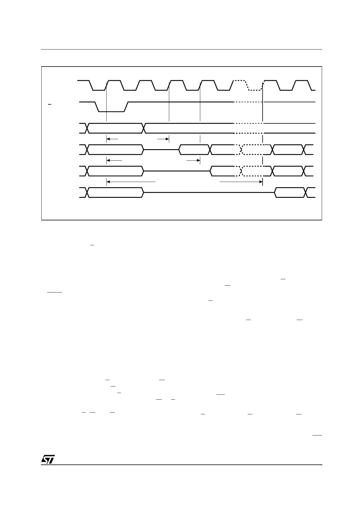
Figure 4. Read Operation Sequence when CR15 = 0 (excluding Read Memory Array)
K
L
A16-A20
ADQ0-ADQ15
ADQ0-ADQ15
ADQ0-ADQ15
VALID ADDRESS
CONF. CODE 2
VALID ADDRESS
VALID DATA NOT VALID
CONFIGURATION CODE 3
VALID ADDRESS
VALID DATA
CONFIGURATION CODE 6
VALID ADDRESS
NOT VALID
NOT VALID
VALID DATA
AI90112
Burst Read. The device also supports a burst
read. In this mode, an address is first latched on
the rising edge of L or K (or falling edge of K, ac-
cording to configuration settings); after a config-
urable delay of 2 to 6 clock cycles a new data is
output at each clock cycle. The burst sequence
may be configured for linear or interleaved order
and for a length of 4, 8 words or for continuous
burst mode.
A WAIT signal may be asserted to indicate to the
system that an output delay will occur.
This delay will depend on the starting address of
the burst sequence; the worst case delay will oc-
cur when the sequence is crossing a 32 word
boundary and the starting address was at the end
of a four word boundary. See the Write Configura-
tion Register (CR) Instruction for more details on
all the possible settings for the synchronous burst
read.
Write. Write operations are used to give Instruc-
tion Commands to the memory or to latch Input
Data to be programmed. A write operation is initi-
ated when Chip Enable E and Write Enable W are
at VIL with Output Enable G at VIH. Addresses are
latched on the rising edge of L. Commands and In-
put Data are latched on the rising edge of W or E
whichever occurs first. Noise pulses of less than
5ns typical on E, W and G signals do not start a
write cycle. Write operations are asynchronous
and clock is ignored during write.
Dual Bank Operations. The Dual Bank allows to
read data from one bank of memory while a pro-
gram or erase operation is in progress in the other
bank of the memory. Read and Write cycles can
be initiated for simultaneous operations in different
banks without any delay. Status Register during
Program or Erase must be monitored using an ad-
dress within the bank being modified.
Output Disable. The data outputs are high im-
pedance when the Output Enable G is at VIH with
Write Enable W at VIH.
Standby. The memory is in standby when Chip
Enable E is at VIH and the P/E.C. is idle. The pow-
er consumption is reduced to the standby level
and the outputs are high impedance, independent
of the Output Enable G or Write Enable W inputs.
Automatic Standby. When in Read mode, after
150ns of bus inactivity and when CMOS levels are
driving the addresses, the chip automatically en-
ters a pseudo-standby mode where consumption
is reduced to the CMOS standby value, while out-
puts still drive the bus. The automatic standby fea-
ture is not available when the device is configured
for synchronous burst mode.
Power-down. The memory is in Power-down
when the Configuration Register is set for Power-
down and RP is at VIL. The power consumption is
reduced to the Power-down level, and Outputs are
in high impedance, independent of the Chip En-
able E, Output Enable G or Write Enable W inputs.
Block Locking. Any combination of blocks can
be temporarily protected against Program or
Erase by setting the lock register and pulling WP
to VIL (see Block Lock instruction).
11/49
Share Link: 