FDD6635 „Éá„Éľ„āŅ„ā∑„Éľ„Éą„ĀģŤ°®Á§ļÔľąPDFÔľČ - Fairchild Semiconductor
ťÉ®ŚďĀÁē™ŚŹ∑
„ā≥„É≥„ÉĚ„Éľ„Éć„É≥„ÉąŤ™¨śėé
„É°„Éľ„āę„Éľ
FDD6635 Datasheet PDF : 8 Pages
| |||
Test Circuits and Waveforms
VDS
VGS
RGEN
0V
VGS
tp
vary tP to obtain
required peak IAS
L
DUT
IAS
0.01ő©
+
VDD
-
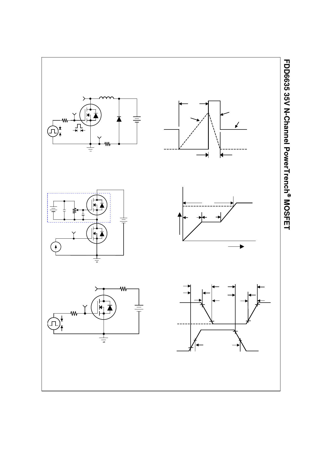
Figure 14. Unclamped Inductive Load Test
Circuit
Drain Current Regulator
Same type as DUT
+
10V
50kő©
-
10őľF
1őľF
VGS
DUT
+
VDD
-
Ig(REF)
tP
IAS
BVDSS
VDS
VDD
tAV
Figure 15. Unclamped Inductive Waveforms
10V
QG
VGS
QGS
QGD
Charge, (nC)
Figure 16. Gate Charge Test Circuit
VDS
VGS
RGEN
VGS Pulse Width ‚ȧ 1őľs
Duty Cycle ‚ȧ 0.1%
RL
DUT
+
VDD
-
Figure 18. Switching Time Test Circuit
Figure 17. Gate Charge Waveform
VDS
tON
td(ON)
tr
90%
tOFF
td(OFF)
tf
90%
0V
VGS
10%
0V
10%
50%
Pulse Width
10%
90%
50%
Figure 19. Switching Time Waveforms
FDD6635 Rev. C2(W)
www.fairchildsemi.com
Share Link: 