HT46R48E データシートの表示(PDF) - Holtek Semiconductor
部品番号
コンポーネント説明
メーカー
HT46R48E Datasheet PDF : 46 Pages
| |||
HT46R48E
stack. After a chip reset, the SP will point to the top of the
stack.
If the stack is full and a non-masked interrupt takes
place, the interrupt request flag will be recorded but the
acknowledgment will be inhibited. When the stack
pointer is decremented (by RET or RETI), the interrupt
will be serviced. This feature prevents stack overflow al-
lowing the programmer to use the structure more easily.
In a similar case, if the stack is full and a ²CALL² is sub-
sequently executed, stack overflow occurs and the first
entry will be lost (only the most recent 6 return ad-
dresses are stored).
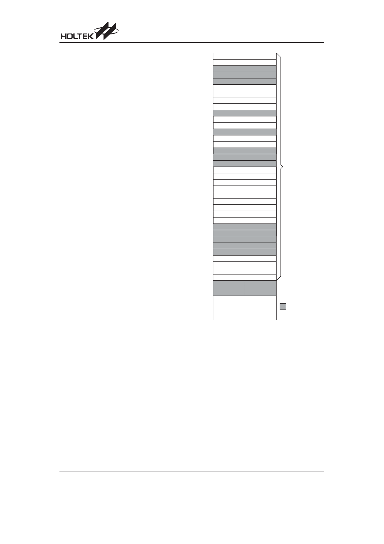
Data Memory - RAM
The data memory is designed with 87´8 bits. The data
memory is divided into two functional groups: special
function registers and general purpose data memory
(64´8). Most are read/write, but some are read only.
The special function registers include the indirect ad-
dressing register (00H), timer/event counter
(TMR;0DH), timer/event counter control register
(TMRC;0EH), program counter lower-order byte regis-
ter (PCL;06H), memory pointer register (MP;01H), ac-
cumulator (ACC;05H), table pointer (TBLP;07H), table
higher-order byte register (TBLH;08H), status register
(STATUS;0AH), interrupt control register (INTC;0BH),
PWM data register (PWM;1AH), the A/D result
lower-order byte register (ADRL;20H), the A/D result
higher-order byte register (ADRH;21H), the A/D control
register (ADCR;22H), the A/D clock setting register
(ACSR;23H), I/O registers (PA;12H, PB;14H, PC;16H,
PD;18H) and I/O control registers (PAC;13H,
PBC;15H, PCC;17H, PDC;19H). The remaining space
before the 40H is reserved for future expanded usage
and reading these locations will get ²00H². The general
purpose data memory, addressed from 40H to 7FH, is
used for data and control information under instruction
commands.
All of the data memory areas can handle arithmetic,
logic, increment, decrement and rotate operations di-
rectly. Except for some dedicated bits, each bit in the
data memory can be set and reset by ²SET [m].i² and
²CLR [m].i². They are also indirectly accessible through
memory pointer register (MP;01H).
Indirect Addressing Register
Location 00H is an indirect addressing register that is
not physically implemented. Any read/write operation of
[00H] accesses data memory pointed to by MP (01H).
Reading location 00H itself indirectly will return the re-
sult 00H. Writing indirectly results in no operation.
The memory pointer register MP (01H) is a 7-bit register.
The bit 7 of MP is undefined and reading will return the
result ²1². Any writing operation to MP will only transfer the
lower 7-bit data to MP.
00H
In d ir e c t A d d r e s s in g R e g is te r
01H
MP
02H
03H
04H
05H
ACC
06H
PCL
07H
TB LP
08H
TB LH
09H
0A H
STATU S
0B H
IN T C
0C H
0D H
TM R
0E H
TM R C
0FH
10H
11H
12H
PA
13H
PAC
14H
PB
15H
PBC
16H
PC
17H
PCC
18H
PD
19H
PDC
1A H
PW M
1B H
1C H
1D H
1E H
1FH
20H
ADRL
21H
ADRH
22H
ADCR
23H
ACSR
24H
S p e c ia l P u r p o s e
D a ta M e m o ry
3FH
40H
G e n e ra l P u rp o s e
D a ta M e m o ry
:U nused
(6 4 B y te s )
R e a d a s "0 0 "
7FH
RAM Mapping
Accumulator
The accumulator is closely related to ALU operations. It
is also mapped to location 05H of the data memory and
can carry out immediate data operations. The data
movement between two data memory locations must
pass through the accumulator.
Arithmetic and Logic Unit - ALU
This circuit performs 8-bit arithmetic and logic opera-
tions. The ALU provides the following functions:
· Arithmetic operations (ADD, ADC, SUB, SBC, DAA)
· Logic operations (AND, OR, XOR, CPL)
· Rotation (RL, RR, RLC, RRC)
· Increment and Decrement (INC, DEC)
· Branch decision (SZ, SNZ, SIZ, SDZ ....)
Rev. 1.10
9
March 24, 2006
Share Link: 