IDT49C460 データシートの表示(PDF) - Integrated Device Technology
部品番号
コンポーネント説明
メーカー
IDT49C460 Datasheet PDF : 32 Pages
| |||
IDT49C460/A/B/C/D/E
32-BIT CMOS ERROR DETECTION AND CORRECTION UNIT
MILITARY AND COMMERCIAL TEMPERATURE RANGES
32-BIT DATA WORD CONFIGURATION
A single IDT49C460 EDC unit, connected as shown in
Figure 1, provides all the logic needed for single bit error
correction and double bit error detection of a 32-bit data field.
The identification code indicates 7 check bits are required.
The CB7 pin should be HIGH.
Figure 3 indicates the 39-bit data format for two bytes of
data and 7 check bits. Table 3 describes the operating mode
available.
Table 6 indicates the data bits participating in the check bit
generation. For example, check bit C0 is the exclusive-OR
function of the 16 data input bits marked with an X. Check bits
are generated and output in the Generate and Initialization
Mode. Check bits from the respective latch are passed,
unchanged, in the PASSTHRU or Diagnostic Generate Mode.
Syndrome bits are generated by an exclusive-OR or the
generated check bits with the read check bits. For example,
Sn is the XOR of check bits Cn from those read with those
generated. Table 7 indicates the decoding of the seven
syndrome bits to identify the bit-in-error for a single bit error,
or whether a double or triple bit error was detected. The all
zero case indicates no errors detected.
In the Correct Mode, the syndrome bits are used to
complement (correct) single bit errors in the data bits. For
double or multiple error detection, the data available as input
to the Data Out Latch is not defined.
Table 5 defines the bit definition for the Diagnostic Latch.
As defined in Table 3, several modes will use the diagnostic
check bits to determine syndrome bits or to pass as check bits
to the SC0–7 outputs. The Internal Mode substitutes the
indicated bit position for the external control signals.
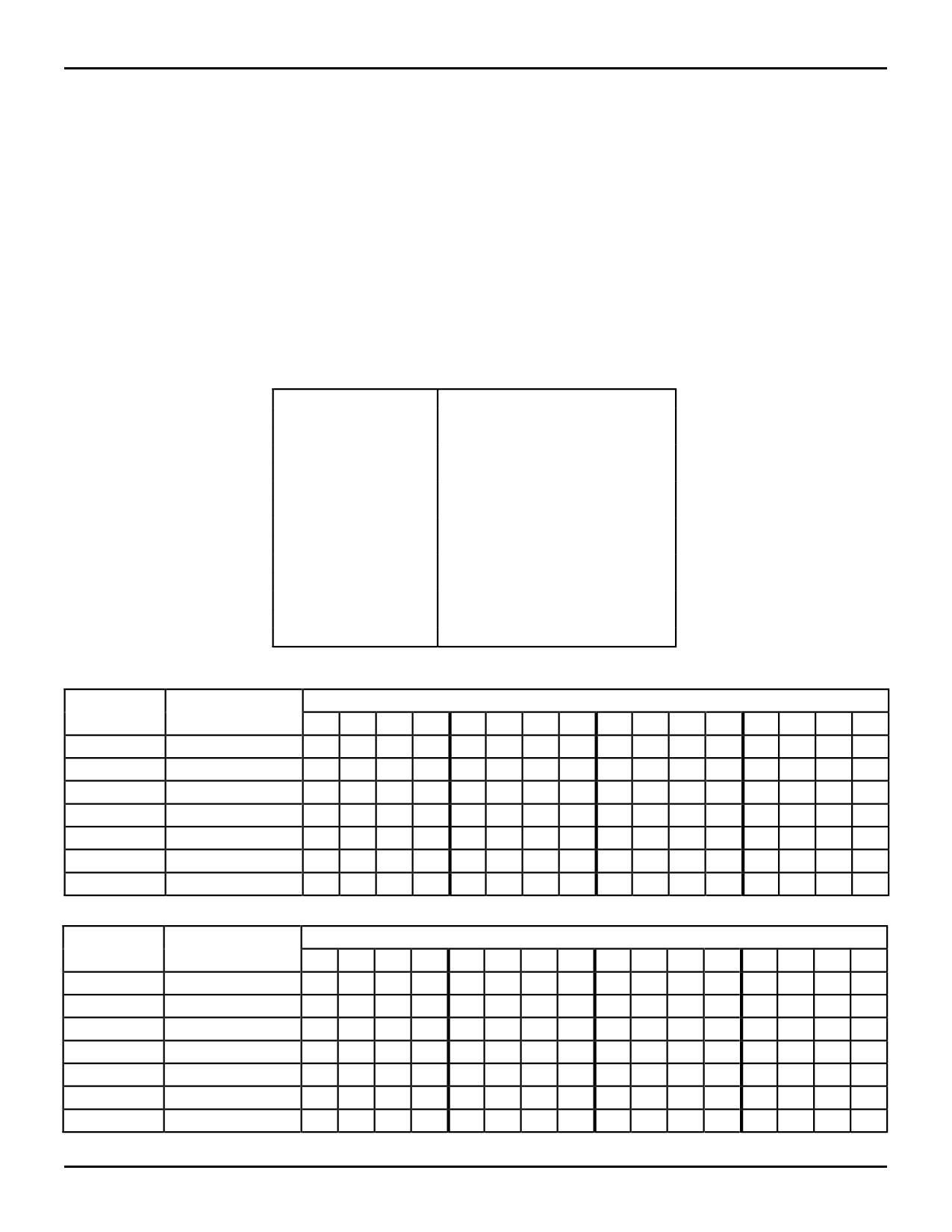
BIT 0
BIT 1
BIT 2
BIT 3
BIT 4
BIT 5
BIT 6
BIT 7
BIT 8
BIT 9
BIT 10
BIT 11
BIT 12
BIT 13–31
CB0 DIAGNOSTIC
CB1 DIAGNOSTIC
CB2 DIAGNOSTIC
CB3 DIAGNOSTIC
CB4 DIAGNOSTIC
CB5 DIAGNOSTIC
CB6 DIAGNOSTIC
CB7 DIAGNOSTIC
CODE ID0
CODE ID1
DIAG MODE0
DIAG MODE1
CORRECT
DON'T CARE
2584 drw 05
Table 5. 32-Bit Diagnostic Latch Coding Format
Generated
Check Bits
C0
C1
C2
C3
C4
C5
C6
Parity
Even (XOR)
Even (XOR)
Odd (XNOR)
Odd (XNOR)
Even (XOR)
Even (XOR)
Even (XOR)
Participating Data Bits
0 1 2 3 4 5 6 7 8 9 10 11 12 13 14 15
X
X
X X XX
X
X
XXX
X
X
X
X
X
X
XX
X
XX
X
X
XX
XXX
X XX
X X XX X X
XX
XX X X XX X X
X X X X XX X X
2584 tbl 06
Generated
Check Bits
C0
C1
C2
C3
C4
C5
C6
Participating Data Bits
Parity
16 17 18 19 20 21 22 23 24 25 26 27 28 29 30 31
Even (XOR)
XXX
X
X
XX
X
Even (XOR)
XXX
X
X
X
X
X
Odd (XNOR)
X
XX
X
XX
X
X
Odd (XNOR)
XX
XXX
X XX
Even (XOR)
X X XX X X
XX
Even (XOR)
XX X X XX X X
Even (XOR)
XX X X XX X X
Table 6. 32–Bit Modified Hamming Code–Check Bit Encode Chart
2584 tbl 07
11.6
9
Share Link: 