LT3579IUFD-1-PBF データシートの表示(PDF) - Linear Technology
部品番号
コンポーネント説明
メーカー
LT3579IUFD-1-PBF Datasheet PDF : 40 Pages
| |||
LT3579/LT3579-1
OPERATION
When a fault is detected, in addition to the FAULT pin
being pulled low internally, the LT3579 also disables
its CLKOUT pin, turns off its power switches, and the
GATE pin becomes high impedance (refer to the State
Diagram). The external PMOS, M1, turns off when the
gate of M1 is pulled up to its source by the external
RGATE resistor (see Block Diagram) With the external
PMOS turned off, the power path from VIN to VOUT is
cut off, protecting power components downstream.
At the same time, a timeout sequence commences where
the SS pin is charged up to 1.8V (the SS pin will continue
charging up to ~2.1V and be held there in the case of
a FAULT1 event still existing), and then discharged to
50mV. This timeout period relieves the part, the PMOS,
and other downstream power components from electrical
and thermal stress for a minimum amount of time as set
by the voltage ramp rate on the SS pin.
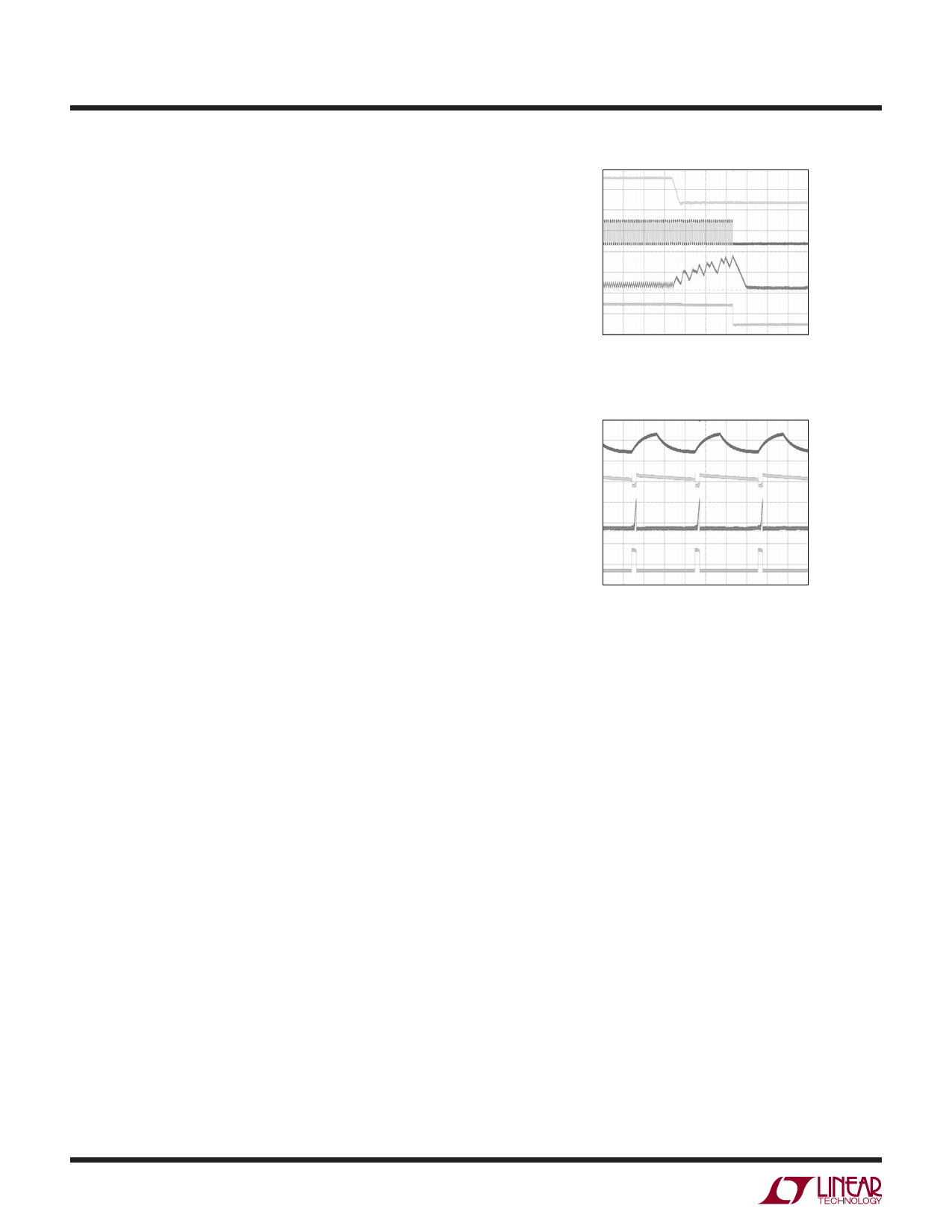
In the absence of faults, the FAULT pin is pulled high by
the external RFAULT resistor (typically 100k). Figures 4
and 5 show the events that accompany the detection of
an output short on the LT3579.
VOUT
10V/DIV
CLKOUT
2V/DIV
IL
5A/DIV
FAULT
5V/DIV
10μs/DIV
35791 F04
Figure 4. Output Short Circuit Protection of the LT3579
SS
2V/DIV
GATE
5V/DIV
IL
5A/DIV
FAULT
5V/DIV
50ms/DIV
35791 F05
Figure 5. Continuous Output Short Showing FAULT Timeout Cycle
35791f
12
Share Link: 