LT3579IUFD-1-PBF データシートの表示(PDF) - Linear Technology
部品番号
コンポーネント説明
メーカー
LT3579IUFD-1-PBF Datasheet PDF : 40 Pages
| |||
LT3579/LT3579-1
APPLICATIONS INFORMATION
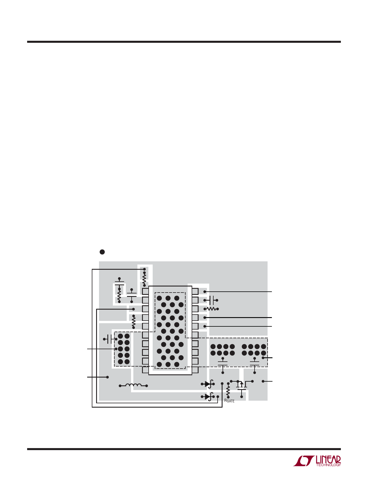
LAYOUT GUIDELINES FOR BOOST, SEPIC, AND DUAL
INDUCTOR INVERTING TOPOLOGIES
• Place the bypass capacitor for the inductor (CPWR) as
close as possible to the inductor.
General Layout Guidelines
• To optimize thermal performance, solder the exposed
ground pad of the LT3579 to the ground plane with
multiple vias around the pad connecting to additional
ground planes.
• A ground plane should be used under the switcher circuitry
to prevent interplane coupling and overall noise.
• Bypass capacitors, CPWR and CVIN, may be combined
into a single bypass capacitor, CIN, if the input side of the
inductor can be close to the VIN pin of the LT3579.
• The load should connect directly to the positive and
negative terminals of the output capacitor for best load
regulation.
Boost Topology Specific Layout Guidelines
• Highspeedswitchingpath(seespecifictopologybelowfor
more information) must be kept as short as possible.
• The VC, FB, and RT components should be placed as
close to the LT3579 as possible, while being as far
away as practically possible from the switch node. The
ground for these components should be separated from
the switch current path.
• Place the bypass capacitor for the VIN pin (CVIN) as
close as possible to the LT3579.
• Keep length of loop (high speed switching path)
governing switch, diode D1, output capacitor COUT, and
ground return as short as possible to minimize parasitic
inductive spikes at the switch node during switching.
SEPIC Topology Specific Layout Guidelines
• Keep length of loop (high speed switching path) governing
switch,flyingcapacitorC1,diodeD1,outputcapacitorCOUT,
and ground return as short as possible to minimize parasitic
inductive spikes at the switch node during switching.
VIAS TO GROUND PLANE REQUIRED TO IMPROVE
THERMAL PERFORMANCE
GND
16
1
21
20
2
19
3
18
4
17
5
16
CIN
6
15
7
14
–
A
B
8
13
VIN
9
10
+
L1
12 COUT1
11
D1
COUT
M1
SYNC
SHDN
CLKOUT
–
VOUT
+
D2
RGATE
3579 F08
A– RETURN CIN GROUND DIRECTLY TO LT3579 EXPOSED PAD PIN 21. IT IS ADVISED TO NOT COMBINE CIN GROUND
WITH GND EXCEPT AT THE EXPOSED PAD.
B– RETURN COUT AND COUT1 GROUND DIRECTLY TO LT3579 EXPOSED PAD PIN 21. IT IS ADVISED TO NOT COMBINE
COUT AND COUT1 GROUND WITH GND EXCEPT AT THE EXPOSED PAD.
Figure 9. Suggested Component Placement for Boost Topology in FE20 Package
35791f
Share Link: 